On Chimera QC Ultra it runs 28x faster than DSP+NPU
ConvNext is one of today’s leading new ML networks. Frankly, it just doesn’t run on most NPUs. So if your AI/ML solution relies on an NPU plus DSP for fallback, you can bet ConvNext needs to run on that DSP as a fallback operation. Our tests of expected performance on a DSP + NPU is dismal – less than one inference per second trying to run the ConvNext backbone if the novel Operators – GeLu and LayerNorm – are not present in the hardwired NPU accelerator and instead those Ops ran on the largest and most powerful DSP core on the market today.
This poor performance makes most of today’s DSP + NPU silicon solutions obsolete. Because that NPU is hardwired, not programmable, new networks cannot efficiently be run.
So what happens when you run ConvNext on Quadric’s Chimera QC Ultra GPNPU, a fully programmable NPU that eliminates the need for a DSP for fallback? The comparison to the DSP-NPU Fallback performance is shocking: Quadric’s Chimera QC Ultra GPNPU is 28 times faster (28,000%!) than the DSP+NPU combo for the same large input image size: 1600 x 928. This is not a toy network, but a real useful image size. And Quadric has posted results for not just one but three different variants of the ConvNext: both Tiny and Small variants, and with input image sizes at 640x640, 800x800, 928x1600. The results are all available for inspection online inside the Quadric Developers’ Studio.
Fully Compiled Code Worked Perfectly
Why did we deliver three different variants of ConvNext all at one time? And why were those three variants added to the online DevStudio environment at the same time as more than 50 other new network examples a mere 3 months (July 2024) after our previous release (April)? Is it because Quadric has an army of super-productive data scientists and low-level software coders who sat chained to their computers 24 hours a day, 7 days a week? Or did the sudden burst of hundreds of new networks happen because of major new feature improvements in our market-leading Chimera Graph Compiler (CGC)? Turns out that it is far more productive – and ethical - for us to build world-class graph compilation technology rather than violate labor laws.
Our latest version of the CGC compiler fully handles all the graph operators found in ConvNext, meaning that we are able to take model sources directly from the model repo on the web and automatically compile the source model to target our Chimera GPNPU. In the case of ConvNext, that was a repo on Github from OpenMMLab with a source Pytorch model. Login to DevStudio to see the links and sources yourself! Not hand-crafted. No operator swapping. No time-consuming surgical alteration of the models. Just a world-class compilation stack targeting a fully-programmable GPNPU that can run any machine learning model.
Lots of Working Models
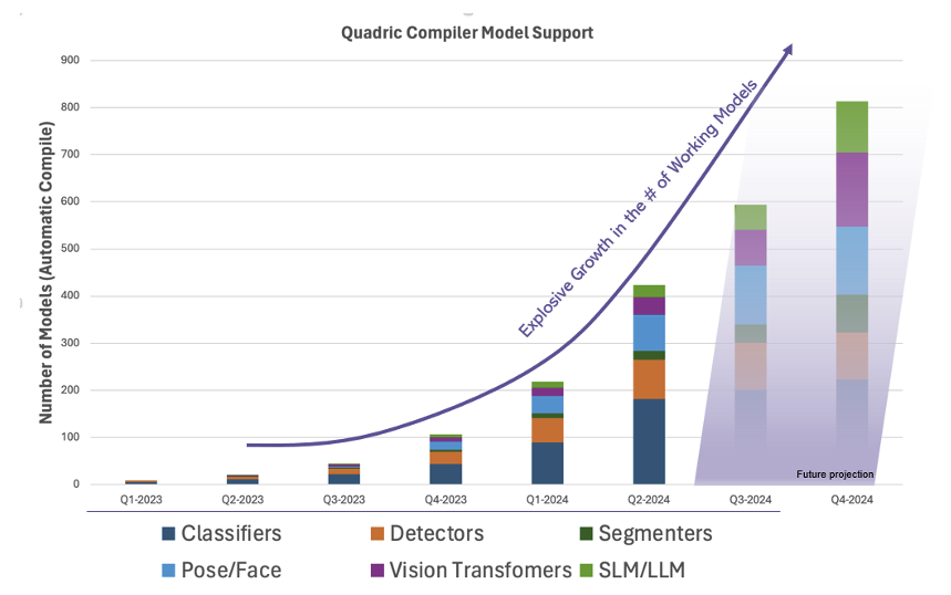
Perhaps more impressive than our ability to support ConvNext – at a high 28 FPS frame rate – is the startling increase in the sheer number of working models that compile and run on the Chimera processor as our toolchain rapidly matures (see chart).
Faster Code, Too
Not only did we take a huge leap forward in the breadth of model support in this latest software release, but we also continue to deliver incremental performance improvements on previous running models as the optimization passes inside the CGC compiler continue to expand and improve. Some networks saw improvements of over 50% in just the past 3 months. We know our ConvNext numbers will rapidly improve.
The performance improvements will continue to flow in the coming months and years as our compiler technology continues to evolve and mature Unlike a hardwired accelerator with fixed feature sets and fixed performance the day you tape-out, a processor can continue to improve as the optimizations and algorithms in the toolchain evolve.
Programmability Provides Futureproofing
By merging the best attributes of dataflow array accelerators with full programmability, Quadric delivers high ML performance while maintaining endless programmability. The basic Chimera architecture pairs a block of multiply-accumulate (MAC) units with a full-function 32-bit ALU and a small local memory. This MAC-ALU-memory building block – called a processing element (PE) - is then tiled into a matrix of PEs to form a family of GPNPUs offering from 1 TOP to 864 TOPs. Part systolic array and part DSP, the Chimera GPNPU delivers what others fails to deliver – the promise of efficiency and complete futureproofing.
What’s the biggest challenge for AI/ML? Power consumption. How are we going to meet it? In late April 2024, a novel AI research paper was published by researchers from MIT and CalTech proposing a fundamentally new approach to machine learning networks – the Kolmogorov Arnold Network – or KAN. In the two months since its publication, the AI research field is ablaze with excitement and speculation that KANs might be a breakthrough that dramatically alters the trajectory of AI models for the better – dramatically smaller model sizes delivering similar accuracy at orders of magnitude lower power consumption – both in training and inference.
However, most every semiconductor built for AI/ML can’t efficiently run KANs. But we Quadric can.
First, some background.
The Power Challenge to Train and Infer
Generative AI models for language and image generation have created a huge buzz. Business publications and conferences speculate on the disruptions to economies and the hoped-for benefits to society. But also, the enormous computational costs to training then run ever larger model has policy makers worried. Various forecasts suggest that LLMs alone may consume greater than 10% of the world’s electricity in just a few short years with no end in sight. No end, that is, until the idea of KANs emerged! Early analysis suggests KANs can be 1/10th to 1/20th the size of conventional MLP-based models while delivering equal results.
Note that it is not just the datacenter builder grappling with enormous compute and energy requirements for today’s SOTA generative AI models. Device makers seeking to run GenAI in device are also grappling with compute and storage demands that often exceed the price points their products can support. For the business executive trying to decide how to squeeze 32 GB of expensive DDR memory on a low-cost mobile phone in order to be able to run a 20B parameter LLM, the idea of a 1B parameter model that neatly fits into the existing platform with only 4 GB of DDR is a lifesaver!
Built Upon a Different Mathematical Foundation
Today’s AI/ML solutions are built to efficiently execute matrix multiplication. This author is more aspiring comedian than aspiring mathematician, so I won’t attempt to explain the underlying mathematical principles of KANs and how they differ from conventional CNNs and Transformers – and there are already several good, high-level explanations published for the technically literate, such this and this. But the key takeaway for the business-minded decision maker in the semiconductor world is this: KANs are not built upon the matrix-multiplication building block. Instead, executing a KAN inference consists of computing a vast number of univariate functions (think, polynomials such as: [ 8 X3 – 3 X2 + 0.5 X ] and then ADDING the results. Very few MATMULs.
Toss Out Your Old NPU and Respin Silicon?
No Matrix multiplication in KANs? What about the large silicon area you just devoted to a fixed-function NPU accelerator in your new SoC design? Most NPUs have hard-wired state machines for executing matrix multiplication – the heart of the convolution operation in current ML models. And those NPUs have hardwired state machines to implement common activation (such as ReLu and GeLu) and pooling functions. None of that matters in the world of KANs where solving polynomials and doing frequent high-precision ADDs is the name of the game.
GPNPUs to the Rescue
The semiconductor exec shocked to see KANs might be imagined to exclaim, “If only there was a general-purpose machine learning processor that had massively-parallel, general-purpose compute that could perform the ALU operations demanded by KANs!”
But there is such a processor! Quadric’s Chimera GPNPU uniquely blends both the matrix-multiplication hardware needed to efficiently run conventional neural networks with a massively parallel array of general-purpose, C++ programmable ALUs capable of running any and all machine learning models. Quadric’s Chimera QB16 processor, for instance, pairs 8192 MACs with a whopping 1024 full 32-bit fixed point ALUs, giving the user a massive 32,768 bits of parallelism that stands ready to run KAN networks - if they live up to the current hype – or whatever the next exciting breakthrough invention turns out to be in 2027. Future proof your next SoC design – choose Quadric!
Not just a little slow down. A massive failure!
Conventional AI/ML inference silicon designs employ a dedicated, hardwired matrix engine – typically called an “NPU” – paired with a legacy programmable processor – either a CPU, or DSP, or GPU. You can see this type of solution from all of the legacy processor IP licensing companies as they try to reposition their cash-cow processor franchises for the new world of AI/ML inference. Arm offers an accelerator coupled to their ubiquitous CPUs. Ceva offers an NPU coupled with their legacy DSPs. Cadence’s Tensilica team offers an accelerator paired with a variety of DSP processors. There are several others, all promoting similar concepts.
The common theory behind these two-core (or even three core) architectures is that most of the matrix-heavy machine learning workload runs on the dedicated accelerator for maximum efficiency and the programmable core is there as the backup engine – commonly known as a Fallback core – for running new ML operators as the state of the art evolves.
As Cadence boldly and loudly proclaims in a recent blog : “The AI hardware accelerator will provide the best speed and energy efficiency, as the implementation is all done in hardware. However, because it is implemented in fixed-function RTL (register transfer level) hardware, the functionality and architecture cannot be changed once designed into the chip and will not provide any future-proofing.” Cadence calls out NPUs – including their own! - as rigid and inflexible, then extols the virtues of their DSP as the best of the options for Fallback. But as we explain in detail below, being the best at Fallback is sorta like being the last part of the Titanic to sink: you are going to fail spectacularly, but you might buy yourself a few extra fleeting moments to rue your choice as the ship sinks.
In previous blogs, we’ve highlighted the conceptual failings of the Fallback concept. Let’s now drill deeper into an actual example to show just how dreadfully awful the Fallback concept is in real life!
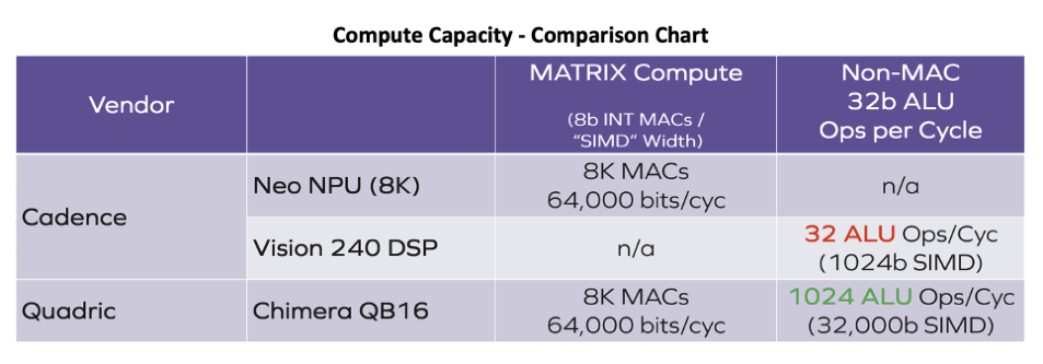
Let’s compare the raw computational capacity of the conventional architecture concept using Cadence’s products as an example versus that of Quadric’s dramatically higher performance Chimera GPNPU. Both the Cadence solution chosen for this comparison and the Quadric solution have 16 TOPs of raw machine learning horsepower – 8K multiply-accumulate units each, clocked at 1 GHz. Assuming both companies employ competent design teams you would be right to assume that both solutions deliver similar levels of performance on the key building block of neural networks – the convolution operation.
But when you compare the general-purpose compute ability of both solutions, the differences are stark. Quadric’s solution has 1024 individual 32bit ALUs yielding an aggregate of 32,000 bits of ALU parallelism, compared to only 1024 bits for the Cadence product. That means any ML function that needs to “fall back” to the DSP in the Cadence solution runs 32 times slower than on the Quadric solution. Other processor vendor NPU solutions are even worse than that! Cadence’s 1024-bit DSP is twice as powerful as simpler 512-bit DSPs or four times as powerful as vector extensions to CPUs that only deliver 256-bit SIMD parallelism. Those other products are 64X or 128X slower than Quadric!
ConvNext – A Specific, Current Day Example
One of the more recent new ML networks is ConvNext, boasting top-1 accuracy levels of as much as 87.8% - nearly 10 full percentage points higher than the Resnet architectures of just a few years ago. Two key layers in the ConvNext family of networks that typically are not present in fixed-function NPUs are the LayerNorm normalization function and the GeLU activation used in place of the previously more common ReLU activation. In the conventional architectures promoted by other IP vendors, the GeLU and LayerNorm operations would run on the FallBack DSP, not the accelerator. The result – shown in the calculations in the illustration below – are shocking!
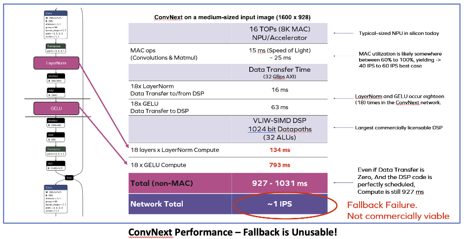
Fallback Fails – Spectacularly
Our analysis of ConvNext on an NPU+DSP architecture suggests a throughput of less than 1 inference per second. Note that these numbers for the fallback solution assume perfect 100% utilization of all the available ALUs in an extremely wide 1024-bit VLIW DSP. Reality would undoubtably be below the speed-of-light 100% mark, and the FPS would suffer even more. In short, Fallback is unusable. Far from being a futureproof safety net, the DSP or CPU fallback mechanism is a death-trap for your SoC.
Is ConvNext an Outlier?
A skeptic might be thinking: “yeah, but Quadric probably picked an extreme outlier for that illustration. I’m sure there are other networks where Fallback works perfectly OK!”. Actually, ConvNext is not an outlier. It only has two layer types requiring fallback. The extreme outlier is provided to us by none other than Cadence in the previously mentioned blog post. Cadence wrote about the SWIN (shifted window) Transformer:
“When a SWIN network is executed on an AI computational block that includes an AI hardware accelerator designed for an older CNN architecture, only ~23% of the workload might run on the AI hardware accelerator’s fixed architecture. In this one instance, the SWIN network requires ~77% of the workload to be executed on a programmable device.”
Per Cadence’s own analysis: 77% of the entire SWIN network would need to run on the Fallback legacy processor. At that rate, why even bother to have an NPU taking up area on the die – just run the entire network – very, very slowly – on a bank of DSPs. Or, throw away your chip design and start over again - if you can convince management to give you the $250M budget for a new tapeout in an advanced node!
Programmable, General Purpose NPUs (GPNPU)
There is a new architectural alternative to fallback – the Chimera GPNPU from Quadric. By merging the best attributes of dataflow array accelerators with full programmability (see last month’s blog for details) Quadric delivers high ML performance while maintaining endless programmability. The basic Chimera architecture pairs a block of multiply-accumulate (MAC) units with a full-function 32bit ALU and a small local memory. This MAC-ALU-memory building block – called a processing element (PE) - is then tiled into a matrix of 64, 256 or 1024 PEs to form a family of GPNPUs offering from 1 TOP to 16 TOPs each, and multicore configurations reaching hundreds of TOPs. Part systolic array and part DSP, the Chimera GPNPU delivers what Fallback fails to deliver – the promise of efficiency and complete futureproofing. See more at quadric.io.
The ResNet family of machine learning algorithms, introduced to the AI world in 2015, pushed AI forward in new ways. However, today’s leading edge classifier networks – such as the Vision Transformer (ViT) family - have Top 1 accuracies a full 10% points of accuracy ahead of the top-rated ResNet in the leaderboard. ResNet is old news. Surely other new algorithms will be introduced in the coming years.
Let’s take a look back at how far we’ve come. Shortly after introduction, new variations were rapidly discovered that pushed the accuracy of ResNets close to the 80% threshold (78.57% Top 1 accuracy for ResNet-152 on ImageNet). This state-of-the-art performance at the time coupled with the rather simple operator structure that was readily amenable to hardware acceleration in SoC designs turned ResNet into the go-to litmus test of ML inference performance. Scores of design teams built ML accelerators in the 2018-2022 time period with ResNet in mind.
These accelerators – called NPUs – shared one common trait – the use of integer arithmetic instead of floating-point math. Integer formats are preferred for on-device inference because an INT8 multiply-accumulate (the basic building block of ML inference) can be 8X to 10X more energy efficient than executing the same calculation in full 32-bit floating point. The process of converting a model’s weights from floating point to integer representation is known as quantization. Unfortunately, some degree of fidelity is always lost in the quantization process.
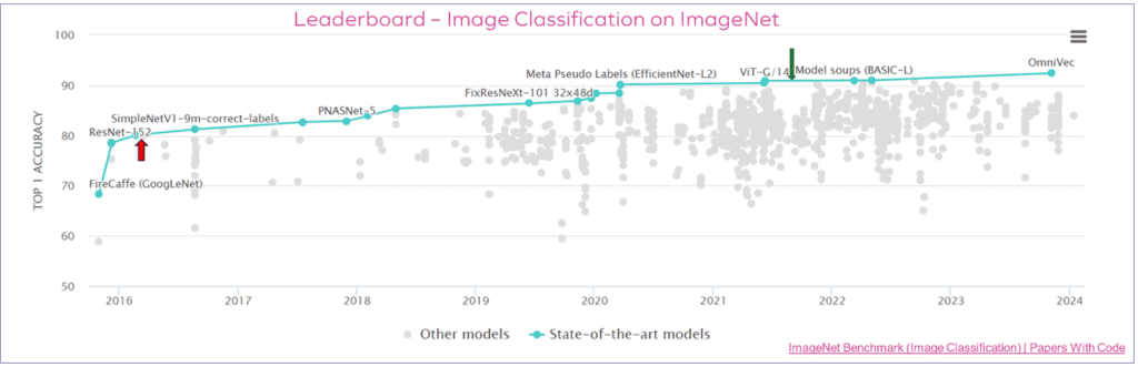
NPU designers have, in the past half-decade, spent enormous amounts of time and energy fine-tuning their weight quantization strategies to minimize the accuracy loss of an integer version of ResNet compared to the original Float-32 source (often referred to as Top-1 Loss). For most builders and buyers of NPU accelerators, a loss of 1% or less is the litmus test of goodness. Some even continue to fixate on that number today, even in the face of dramatic evidence that suggests now-ancient networks like ResNet should be relegated to the dustbin of history. What evidence, you ask? Look at the “leaderboard” for ImageNet accuracy that can be found on the Papers With Code website:
https://paperswithcode.com/sota/image-classification-on-imagenet
It’s Time to Leave the Last Decade Behind
As the leaderboard chart aptly demonstrates, today’s leading edge classifier networks – such as the Vision Transformer (ViT) family - have Top 1 accuracies exceeding 90%, a full 10% points of accuracy ahead of the top-rated ResNet in the leaderboard. For on-device ML inference performance, power consumption and inference accuracy must all be balanced for a given application. In applications where accuracy really matters – such as automotive safety applications –design teams should be rushing to embrace these new network topologies to gain the extra 10+% in accuracy.
It certainly makes more sense to embrace 90% accuracy thanks to a modern ML network – such as ViT, or SWIN transformer, or DETR - rather than fine-tuning an archaic network in pursuit of its original 79% ceiling? Of course. So then why haven’t some teams made the switch?
Why Stay with an Inflexible Accelerator?
Perhaps those who are not Embracing The New are limited because they chose accelerators with limited support of new ML operators. If a team implemented a fixed-function accelerator four years ago in an SoC that cannot add new ML operators, then many newer networks – such as Transformers – cannot run on those fixed-function chips today. A new silicon respin – which takes 24 to 36 months and millions of dollars – is needed.
But one look at the leaderboard chart tells you that picking a fixed-function set of operators now in 2024 and waiting until 2027 to get working silicon only repeats the same cycle of being trapped as new innovations push state-of-the-art accuracy, or retains accuracy with less computational complexity. If only there was a way to run both known networks efficiently and tomorrow’s SOTA networks on device with full programmability!
Use Programmable, General Purpose NPUs (GPNPU) Luckily, there is now an alternative to fixed-function accelerators. Since mid-2023 Quadric has been delivering its Chimera General-Purpose NPU (GPNPU) as licensable IP. With a TOPs range scaling from 1 TOP to 100s of TOPs, the Chimera GPNPU delivers accelerator-like efficiency while maintaining C++ programmability to run any ML operator, and we mean any. Any ML graph. Any new network. Even ones that haven’t been invented yet. Embrace the New!
In today’s disaggregated electronics supply chain the (1) application software developer, (2) the ML model developer, (3) the device maker, (4) the SoC design team and (5) the NPU IP vendor often work for as many as five different companies. It can be difficult or impossible for the SoC team to know or predict actual AI/ML workloads and full system behaviors as many as two or three years in advance of the actual deployment. But then how can that SoC team make good choices provisioning compute engines and adequate memory resources for the unknown future without defaulting to “Max TOPS / Min Area”?
There has to be a smarter way to eliminate bottlenecks while determining the optimum local memory for AI/ML subsystems.
Killer Assumptions
“I want to maximize the MAC count in my AI/ML accelerator block because the TOPs rating is what sells, but I need to cut back on memory to save cost,” said no successful chip designer, ever.
Emphasis on “successful” in the above quote. We’ve heard comments like this many times. Chip architects – or their marketing teams – try to squeeze as much brag-worthy horsepower into a new chip design as they can while holding down silicon cost.
Many SoC teams deploy home-grown accelerators for machine learning inference. Those internal solutions often lack accurate simulation models that can be plugged into larger SoC system simulations, and they need to be simulated at the logic level in Verilog to determine memory access patterns to the rest of the system resources. With slow gate-level simulation speeds, often the available data set gathered is small and limited to one or two workloads profiled. This lack of detailed information can entice designers into several deadly assumptions.
Killer assumption number one is that the memory usage patterns of today’s reference networks – many of which are already five or more years old (think ResNet) - will remain largely unchanged as networks evolve.
The second risky assumption is to simplistically assume a fixed percentage of available system external bandwidth that doesn’t account for resource contention over time.
Falling prey to those two common traps can lead the team to declare design goals have been met with just a small local memory buffer dedicated to the NPU accelerator. Unfortunately, they find out after silicon is in-hand that perhaps newer models have different data access patterns that require smaller, more frequent random accesses to off-chip memory – a real performance killer in systems that perform best with large burst transfers.
If accelerator performance depends on the next activation data element or network weight being ready for computation by your MAC array within a few clock cycles, waiting 1000 cycles to gain access to the DDR channel only to underutilize it with a tiny data transfer can wreak havoc with achievable performance.
Using Big Memory Buffers Might Not Solve the Problem
You might think the obvious remedy to the conundrum is to provision more SRAM on chip as buffer memory than the bare minimum required. That might help in some circumstances. Or it might just add cost but not solve the problem if a hardwired state machine accelerator with inflexible memory access and stride patterns continues to request an excessive number of tiny block transfer requests to DDR on the chip’s AXI fabric.
The key to finding the Goldilocks amount of memory – not too small and not too much – is twofold:
Solving the Memory Challenge - Smartly
Quadric has written extensively on techniques that analyze data usage across large swathes of an ML graph to ease memory bottlenecks. Our blog on advanced operator fusion – Fusion In Local Memory (FILM) – illustrates these techniques.
Additionally, the extensive suite of system simulation capability that accompanies the Chimera core provides a rich set of data that helps the SoC designer understand code and memory behavior. And the ability of the Chimera Graph Compiler to smartly schedule prefetching of data provides tremendous resiliency to aberrant system response times, even when a Chimera GPNPU is configured with relatively small local memories.
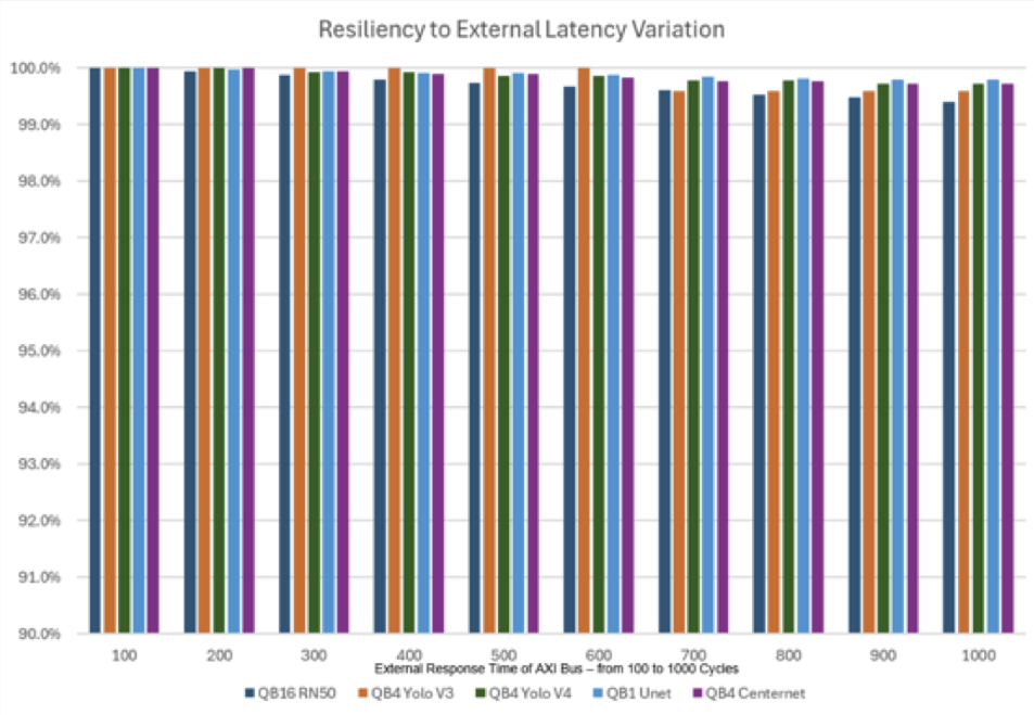
Quadric Chimera GPNPUs can be configured with a local buffer memory ranging from 1 MB to 32 MB, depending on system requirements. Some chip architects assume that a fully C++ programmable processor like the Chimera core needs “large” local memories to deliver good performance. But as the chart below shows, smartly managing local memory with a code-driven graph compilation technology delivers excellent resiliency to system resource contention with even very small local memory configuration.
For this analysis we sampled five different ML networks (ResNet50, two Yolo variants, UNet and CenterNet) across all three Chimera core sizes (1 TOP, 4 TOP, 16 TOP). In all scenarios we modeled core performance with a relatively small 4 MB of local SRAM (called L2 memory in our architecture) and assumed peak AXI system bandwidth to DDR memory of 32 GB/sec (an LPDDR4 or LPDDR5 connection).
Thanks to extensive FILM region optimization and smart data prefetching, all five scenarios show remarkable tolerance of sluggish system response, as the Chimera core performance degrades less than 1% even when average DDR response time is 10X worse than the system ideal of 100 cycles (1000 cycles instead of 100).
The bottom line: Don’t agonize over how much or how little memory to choose. Don’t squeeze memory and simply hope for the best. Choose an ML solution with the kind of programmability, modeling capability, and smart memory management that Quadric offers, and instead of agony, you’ll know you made the right resource choices before you tapeout, and you’ll be saying “Thanks for the memories!” See for yourself at www.quadric.io
Wait! Didn’t That Era Just Begin?
The idea of transformer networks has existed since the seminal publication of the Attention is All You Need paper by Google researchers in June 2017. And while transformers quickly gained traction within the ML research community, and in particular demonstrated superlative results in vision applications (ViT paper), transformer networks were definitely not a topic of trendy conversation around the family holiday dinner table. Until late 2022, that is.
On Nov 30, 2022, OpenAI released ChatGPT and within weeks millions of users were experimenting with it. Soon thereafter the popular business press and even the TV newscasts were both marveling at the results as well as publishing overwrought doomsday predictions of societal upheaval and chaos.
ChatGPT ushered in the importance of Transformer Networks in the world of Machine Learning / AI.
During the first few months of Transformer Fever the large language models (LLMs) based on transformer techniques were the exclusive province of cloud compute centers because model size was much too large to contemplate running on mobile phone, a wearable device, or an embedded appliance. But by the midsummer of 2023 the narrative shifted and in the second half of 2023 every silicon vendor and NPU IP vendor was talking about chip and IP core changes that would support LLMs on future devices.
Change is Constant
Just six weeks after the release of the Llama 2 LLM, Quadric was the first to demonstrate the Llama2 LLM running on an existing IP core in September 2023. But we were quick to highlight that Llama2 wasn’t the end of the evolution of ML models and that hardware solutions needed to be fully programable to react to the massive rate of change occurring in data science. No sooner had that news hit the street – and our target customers in the semiconductor business started ringing our phone off the hook – then we started seeing the same media sources that hyped transformers and LLMs in early 2023 begin to predict the end of the lifecycle for transformers!
Too Early to Predict the End of Transformers?
In September 2023, Forbes was first out of the gate predicting that other ML network topologies would supplant attention-based transformers. Keep in mind, this is a general business-oriented publication aimed at the investor-class, not a deep-tech journal. More niche-focused, ML-centric publications such as Towards Data Science are also piling on, with headlines in December 2023 such as A Requiem For the Transformer.
Our advice: just as doomsday predictions about transformers were too hyperbolic, so too are predictions about the imminent demise of transformer architectures. But make no mistake, the bright minds of data science are hard at work today inventing the Next New Thing that will certainly capture the world’s attention in 2024 or 2025 or 2026 and might one day indeed supplant today’s state of the art.
What Should Silicon Designers Do Today?
Just as today’s ViT and LLM models didn’t completely send last decade’s Resnet models to the junk heap, tomorrow’s new hero model won’t eliminate the LLMs that are consuming hundreds of billions of dollars of venture capital right now. SoC architects need compute solutions that can run last year’s benchmarks (Resnet, etc) plus this year’s hot flavor of the month (LLMs) as well as the unknown future champion of 2026 that hasn’t been invented yet.
Should today’s chip designer choose a legacy hardwired NPU optimized for convolutions? Terrible idea – you already know that first-generation accelerator is broken. Should they adapt and build a second generation, hardwired accelerator evolved to support both CNNs and transformers? No way – still not fully programmable – and the smart architect won’t fall for that trap a second time.
Quadric offers a better way – the Chimera GPNPU. “GP” because it is general purpose: fully C++ programmable to support any innovation in machine learning that comes along in the future. “NPU” because it is massively parallel, matrix-optimized offering the same efficiency and throughput as hardwired “accelerators” but combined with ultimate flexibility. See for yourself at www.quadric.io
It Will Make for a Much Better NPU Vendor Evaluation.
We’ve written before about the ways benchmarks for NPUs can be manipulated to the point where you just can’t trust them. There are two common major gaps in collecting useful comparison data on NPU IP: [1] not specifically identifying the exact source code repository of a benchmark, and [2] not specifying that the entire benchmark code be run end-to-end, with any omissions reported in detail. Our blog explains these gaps.
However, there is a straight-forward, low-investment method to short-circuit all the vendor shenanigans and get a solid apples-to-apples result: Build Your Own Benchmarks. BYOB!
This might sound like a daunting task, but it isn’t. At the very beginning of your evaluation, it’s important to winnow the field of possible NPU vendors. This winnowing is essential now that a dozen or more IP companies are offering NPU “solutions.” At this stage, you don’t need to focus on absolute inference accuracy as much as you need to judge key metrics of [1] performance, [2] memory bandwidth, [3] breadth of NN model support; [4] breadth of NN operator support; and [5] speed and ease of porting of new networks using the vendors’ toolsets. Lovingly crafted quantization can come later.
The Problem with Most ML Reference Models
All machine learning models begin life in a model training framework using floating point data representation. The vast majority of published reference models are found in their native FP32 format – because it’s easy for the data science teams that invent the latest, greatest model to simply publish the original source. But virtually all device-level inference happens in quantized, INT-8 or mixed INT-8/16 formats on energy-optimized NPUs, GPNPUs, CPUs and GPUs that perform model inference at 5X to 10X lower energy than a comparable FP32 version of the same network.
Quantizing FP32 models to INT8 in a manner that preserves inference accuracy can be a daunting prospect for teams without spare data scientists looking for something to keep them busy. But do you really need a lovingly crafted, high-accuracy model to judge the merits of 10 vendor products clamoring for your attention? In short, the answer is: NO.
First, recognize that the benchmarks of today (late 2023, early 2024) are not the same workloads that your SoC will run in 2026 or 2027 when it hits the market – so any labor spent fine-tuning model weights today is likely wasted effort. Save that effort for perhaps a final step in the IP vendor selection, not early in the process.
Secondly, note that the cycle counts and memory traffic data that will form the basis for your PPA (power, performance, area) conclusions will be exactly the same whether the model weights were lovingly hand-crafted or simply auto-converted. What matters for the early stages of an evaluation are: can the NPU run my chosen network? Can it run all the needed operators? What is the performance?
Making Your Own Model
Many IP vendors have laboriously hand-tuned, hand-pruned and twisted a reference benchmark beyond recognition in order to win the benchmark game. You can short-circuit that gamesmanship by preparing your own benchmark model. Many training toolsets have existing flows that can convert floating point models to quantized integer versions. (e.g TensorFlow QAT; Pytorch Quantization). Or you can utilize interchange formats, such as ONNX Runtime, to do the job. Don’t worry about how well the quantization was performed – just be sure that all layers have been converted to an Integer format.
Even if all you do is take a handful of the common networks with some variety – for example: Resnet50, an LLM, VGG16, Vision Transformer, and a Pose network – you can know that the yardstick you give to the IP vendor is the same for all vendors. Ask them to run the model thru their tools and give you both the performance results and the final form of the network they ran to double-check that all of the network ran on the NPU – and none of the operators had to fallback onto a big, power-guzzling CPU.
Better yet – ask the vendor if their tools are robust enough to let you try to run the models yourself!
Getting the Information That Really Counts
BYOB will allow you to quickly ascertain the maturity of a vendor toolchain, the breadth of operator coverage, and the PPA metrics you need to pare that list of candidates down to a Final Two that deserve the full, deep inspection to make a vendor selection.
If you’d like to try running your own benchmarks on Quadric’s toolchain, we welcome you to register for an account in our online Developer’s Studio and start the process! Visit us at www.quadric.io
Llama2, YOLO Family and MediaPipe family of networks now available
October 31, 2023
Quadric today delivered a Halloween treat for all registered users of the Quadric Developers’ Studio. (Link). This latest update of the industry’s flagship GPNPU software tools showcases a significant new batch of machine learning benchmark networks and several big enhancements to the underlying ChimeraTM software development toolkit that powers Quadric’s Chimera general purpose neural processor.
Llama2 Code Available
Quadric’s first to market implementation of the Llama2 large language model is now available for customer viewing and inspection in the benchmarks section of the Studio. Users can explore all aspects of the implementation of the 15M parameter “baby” Llama2 implementation, including all source codes.
MediaPipe Network Family, Yolo Networks
A suite of the Google Mediapipe family of networks is now available: Hand Landmark (full, lite); Palm Detection (Full, Lite); Face Landmark; Face Detection short range; and SSDLite Object Detection all run on the Chimera GPNPU and can be benchmarked and viewed by prospective licensees.
Additionally, full implementations of the YOLO V3 and YOLO V4 networks are also released to DevStudio users. These YOLO model ports are of the complete YOLO networks – all layers, all operators – running entirely on the Chimera GPNPU processor. As with all networks that have been ported to the Chimera family of GPNPUs (spanning a range from 1 TOPs to 16 TOPs) the entire network always runs 100% on the GPNPU and there is no companion CPU or DSP required.
Significant Compiler and Tool Advancements in Chimera SDK 23.10 Release
The quality and performance of code generated by the Chimera Graph Compiler and Chimera C++ compiler continues to make substantial strides with each release. This latest SDK release adds a further 33% performance improvement to Quadric’s already market-leading performance levels on the ViT_B vision transformer, and a 13% performance improvement on the older RESNET18 benchmark network. A full performance improvement chart showing the speedups for more than a dozen networks is available inside DevStudio.
A host of new and enhanced code development and debug tools are also now available to further speed the porting and debug process including a new tool for numerical validation/correlation of accuracy of results between Chimera code and ONNX runtime results, and enhanced performance visualization tools at both the operator and subgraph levels.
Immediate Availability
Current and prospective users can access these new features and benchmarks at https://studio.quadric.io/login
Your Spreadsheet Doesn’t Tell the Whole Story.
Thinking of adding an NPU to your next SoC design? Then you’ll probably begin the search by sending prospective vendors a list of questions, typically called an RFI (Request for Information) or you may just send a Vendor Spreadsheet. These spreadsheets ask for information such as leadership team, IP design practices, financial status, production history, and – most importantly – performance information, aka “benchmarks”.
It's easy to get benchmark information on most IP – these benchmarks are well understood. For an analog I/O cell you might collect jitter specs. For a specific 128-pt complex FFT on a DSP there’s very little wiggle room for the vendor to shade the truth. However, it’s a real challenge for benchmarks for machine learning inference IP, which is usually called an NPU or NPU accelerator.
Why is it such a challenge for NPUs? There are two common major gaps in collecting useful “apples to apples” comparison data on NPU IP: [1] not specifically identifying the exact source code repository of a benchmark, and [2] not specifying that the entire benchmark code be run end to end, with any omissions reported in detail.
Specifying Which Model
It’s not as easy as it seems. Handing an Excel spreadsheet to a vendor that asks for “Resnet50 inferences per second” presumes that both parties know exactly what “Resnet50” means. But does that mean the original Resnet50 from the 2015 published paper? Or from one of thousands of other source code repos labeled “Resnet50”?
The original network was trained using FP32 floating point values. But virtually every embedded NPU runs quantized networks (primarily INT8 numerical formats, some with INT4, INT16 or INT32 capabilities as well.) which means the thing being benchmarked cannot be “the original” Resnet50. Who should do the quantization – the vendor or the buyer? What is the starting point framework – a PyTorch model, a TensorFlow Model, TFLite, ONNX – or some other format? Is pruning of layers or channels allowed? Is the vendor allowed to inject sparsity (driving weight values to zero in order to “skip” computation) into the network? Should the quantization be symmetric, or can asymmetric methods be used?
You can imagine the challenge of comparing the benchmark from vendor X if they use one technique but Vendor Y uses another. Are the model optimization techniques chosen reflective of what the actual users will be willing and able to perform three years later on the state-of-the-art models of the day when the chip is in production? Note that all of these questions are about the preparation of the model input that will flow into the NPU vendor’s toolchain. The more degrees of freedom that you allow an NPU vendor to exploit, the more the comparison yardstick changes from vendor to vendor.
Figure 1. So many benchmark choices.
Using the Entire Model
Once you get past the differences in source models there are still more questions. You need to ask [a] does the NPU accelerator run the entire model – all layers - or does the model need to be split with some graph layers running on other processing elements on chip, and [b] do any of the layers need to be changed to conform to the types of operators supported by the NPU?
Most NPUs implement only a subset of the thousands of possible layers and layer variants found in modern neural nets. Even for old benchmark networks like Resnet50 most NPUs cannot perform the final SoftMax layer computations needed and therefore farm that function out to a CPU or a DSP in what NPU vendors typically call “fallback”.
This Fallback limitation magnifies tenfold when newer transformer networks (Vision Transformers, LLMs) that employ dozens of NMS or Softmax layer types are the target. One of the other most common limitations of NPUs is a restricted range of supported convolution layer types. While virtually all NPUs very effectively support 1x1 and 3x3 convolutions, many do not support larger convolutions or convolutions with unusual strides or dilations. If your network has an 11x11 Conv with Stride 5, do you accept that this layer needs to Fallback to the slower CPU, or do you have to engage a Data Scientist to alter the network to use one of the known Conv types that the high-speed NPU can support?
Taking both of these types of changes into consideration, you need to carefully look at the spreadsheet answer from the IP vendor and ask “Does this Inferences/Sec benchmark data include the entire network, all layers? Or is there a workload burden on my CPU that I need to measure as well?”
Power benchmarks also are impacted: the more the NPU offloads back to the CPU, the better the NPU vendor’s power numbers look – but the actual system power numbers look far, far worse once CPU power and system memory/bus traffic power numbers are calculated.
Gathering and analyzing all the possible variations from each NPU vendor can be challenging, making true apples to apples comparisons almost impossible using only a spreadsheet approach.
The Difference with a Quadric Benchmark
Not only is the Quadric general purpose NPU (GPNPU) a radically different product – running the entire NN graph plus pre- and post-processing C++ code – but Quadric’s approach to benchmarks is different also. Quadric pushes the Chimera toolchain out in the open for customers to see at www.Quadric.io. Our DevStudio includes all the source code for all the benchmark nodes shown, including links back to the source repos. Evaluators can run the entire process from start to finish – download the source graph, perform quantization, compile a graph using our Chimera Graph Compiler and LLVM C++ compilers, and run the simulation to recreate the results. No skipping layers. No radical network surgery, pruning or operator changes. No removal of classes. The full original network with no cheating. Can the other vendors say the same?
In July of 1887, Carl Benz held the first public outing for his “vehicle powered by a gas engine” – the first automobile ever invented. Nine short months after the first car was publicly displayed, the first auto race was staged on April 28, 1887 and spanned a distance of 2 kilometres (1.2 mi) from Neuilly Bridge to the Bois de Boulogne in Paris.
As cars became more dependable and commonplace as a means of convenient transportation, so too grew the desire to discover the technology’s potential. Auto racing formally became an organized sport in the early 1900’s and today it’s a multi-billion dollar per year industry and has produced vehicles capable of max speeds of almost 500kph (over 300mph).
Similar to that first auto race, Artificial Intelligence (AI) applications are in their nascent years, but many are speculating that their impact may be even greater than that of the automobile and many are racing to test their current limits. Similar to how race cars today look nothing like the original three-wheeled Motor Car, AI platforms are changing to meet the performance demands of this new class of programs.
If you’ve been following any of the companies that are joining this race, you may have heard them use the term “operator fusion“ when bragging about their AI acceleration capabilities. One of the most brag-worthy features to come out of the PyTorch 2.0. release earlier this year was the ‘TorchInductor’ compiler backend that can automatically perform operator fusion, which resulted in 30-200% runtime performance improvements for some users.
From context, you can probably infer that “operator fusion“ is some technique that magically makes Deep Neural Network (DNN) models easier and faster to execute… and you wouldn’t be wrong. But what exactly is operator fusion and how can I use operator fusion to accelerate my AI inference applications?
AI applications, especially those that incorporate Deep Neural Network (DNN) inference, are composed of many fundamental operations such as Multiply-Accumulate (MAC), Pooling layers, activation functions, etc.
Conceptually, operator fusion (sometimes also referred to as kernel or layer fusion) is an optimization technique for reducing the costs of two or more operators in succession by reconsidering their scope as if they were a single operator.
You intuitively do this type of “fusion“ routinely in your everyday life without much thought. Consider for example that you have two tasks in a given day: going to the office for work and going to the grocery store for this week's groceries.
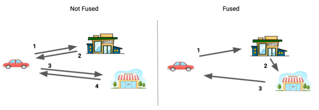
Figure 1. Reducing instances of driving by one by fusing two tasks – “going to work“ and “going to the grocery store“ – by reconsidering them as a single task. Image by Author.
If your office and local grocery store are in the same part of town, you might instinctively stop by the grocery store on your way home from work, reducing the number of legs of your journey by 1 which might result in less total time spent driving and less total distance driven.
Operator fusion intuitively optimizes AI programs in a similar way, but the performance benefits are measured in fewer memory read/writes which results in fewer clock cycles dedicated to program overhead which generates a more efficient program binary.
Let’s look at a practical example. Here’s a visual diagram of a network before and after operator fusion performed by NVIDIA’s TensorRT™ Optimizer:
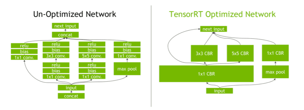
Figure 2. A GoogLeNet Inception module network before and after layer fusion performed by NVIDIA’s TensorRT™ Optimizer. Original image available in this blog post by NVIDIA.
In the example in Figure 2, operator fusion was able to reduce the number of layers (blocks not named “input“ or “next input“) from 20 to 5 by fusing combinations of the following operators:
The performance benefits vary depending on the hardware platform being targeted, but operator fusion can provide benefits for nearly every runtime target. Because of its universality, operator fusion is a key optimization technique in nearly all DNN compilers and execution frameworks.
If reducing the number of kernels reduces program overhead and improves efficiency and these benefits are applicable universally, this might lead us to ask questions like:
To better understand operator fusion's benefits and limitations, let’s take a deeper dive into the problem it’s solving.
Fusing convolutional layers, bias adds, and activation function layers, like NVIDIA’s TensorRT tool did in Figure 2, is an extremely common choice for operator fusion. Convolutions and activation functions can be decomposed into a series of matrix multiplication operations followed by element-wise operations that look something like:
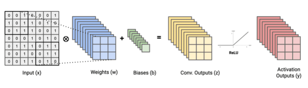
Figure 3. Tensors used in a 3x3 Conv., Bias Add, and ReLU activation function sequence of graph operators. Image by Author.
If these operations are performed in three sequential steps, the graph computation would look something like (left side of Figure 4):
Activation outputs (y) are written to global memory to be used by next operator(s) in the graph
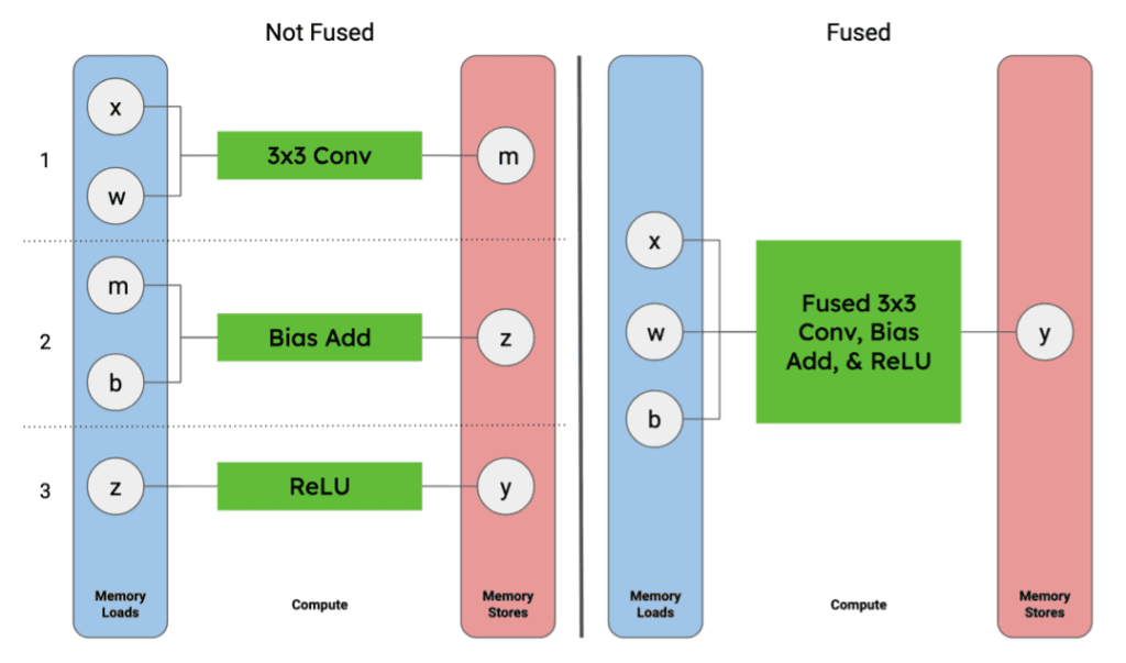
Figure 4. Local memory loads and stores for tensors used in a 3x3 Conv., Bias Add, and ReLU activation function sequence of graph operators compared to a single fused operator. Image by Author.
If the two operations are fused, the graph computation becomes simplified to something like (right side of Figure 4):
By representing these three operations as a single operation, we are able to remove four steps:the need to write and read the intermediate tensor (m) and the convolution output tensor (z) out of and back into local memory. In practice, operator fusion is typically achieved when a platform can keep intermediate tensors in local memory on the accelerator platform.
There are three things that dictate whether the intermediate tensors can remain in local memory:
As we mentioned before, some accelerator platforms are better suited to capitalize on the performance benefits of operator fusion than others. In the next section, we’ll explore why some architectures are more equipped to satisfy these requirements.
DNN models are becoming increasingly deep with hundreds or even thousands of operator layers in order to achieve higher accuracy when solving problems with increasingly broader scopes. As DNNs get bigger and deeper, the memory and computational requirements for running inference also increase.
There are numerous hardware platforms that optimize performance for these compute and memory bottlenecks in a number of clever ways. The benefits of each can be highly subjective to the program(s) being deployed.
We’re going to look at three different types of accelerator cores that can be coupled with a host CPU on a System-on-Chip (SoC) and be targeted for
and see how capable each architecture is of operator fusion:
GPUs, like the Arm Mali-G720, address the memory bottlenecks of AI and abstract the programming complexity of managing memory by using L2 cache. They address the compute bottlenecks by being comprised of general compute cores that operate in parallel, but cannot communicate directly with one another.
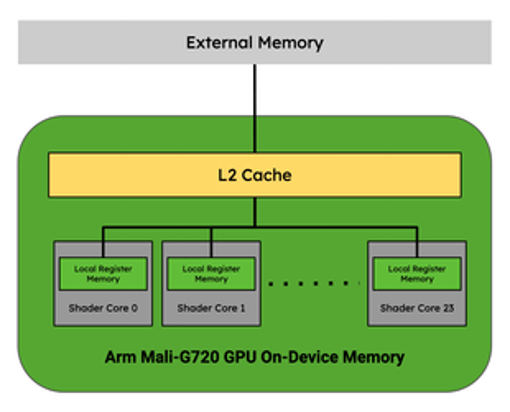
Figure 5. Arm Mali-G720 GPU Memory Hierarchy. Adapted from a diagram in this blog post
In the context of a GPU’s memory hierarchy, operator fusion is possible if the intermediate tensors can fit entirely in the Local Register Memory (LRM) of a given Shader Core without needing to communicate back out to L2 cache.
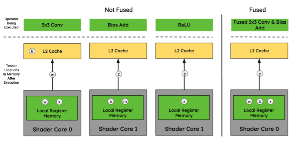
Figure 6. Tensor locations for 3x3 Conv., Bias Add, and ReLU activation function sequence of graph operators in an Arm Mali-G720 GPU memory hierarchy. Image by Author.
Since the GPU cores cannot share data directly with one another, they must write back to L2 Cache in order to exchange intermediate tensor data between processing elements or reorganize to satisfy the requirements of the subsequent operators. This inability to share tensor data between compute cores without writing to and from L2 cache prevents them from fusing multiple convolutions together without duplicating weight tensors across cores which taxes their compute efficiency and memory utilization. Since the memory hierarchy is cache-based, the hardware determines when blocks of memory are evicted or not which can make operator fusion nondeterministic if the available memory is approaching saturation.
For these reasons, GPUs satisfy the compute generality requirement for operator fusion, but are occasionally vulnerable to the memory availability and memory organization requirements.
NPUs, like the Arm Ethos-N78, are customized hardware-accelerator architectures for accelerating AI and, therefore, the way they accelerate AI varies; however the most performant ones today typically use hard-wired systolic arrays to accelerate MAC operations.
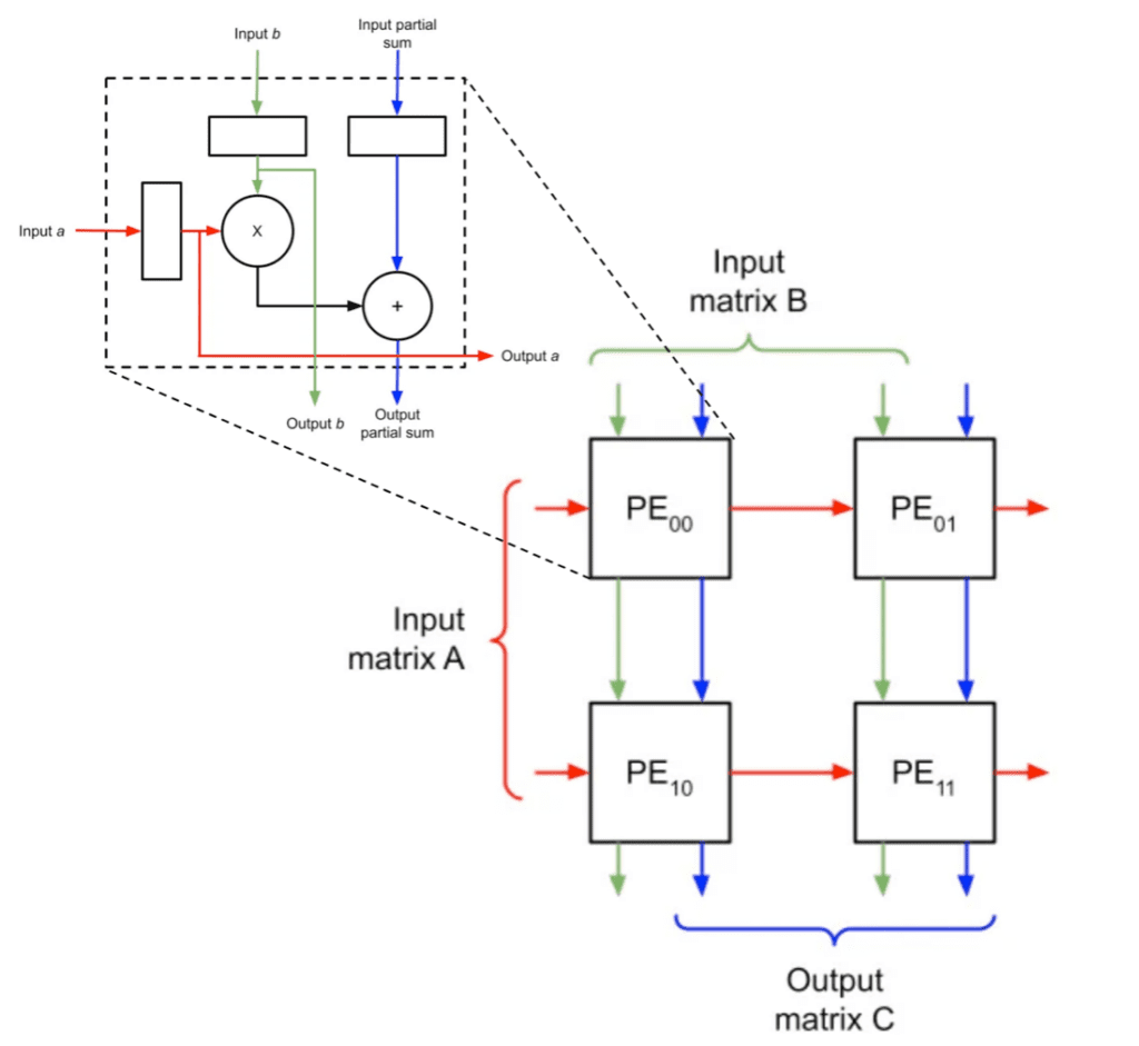
Figure 7. Diagram of a systolic array for MAC operations. Original image adapted from two images in this blog post.
MAC operations are the most frequent and, therefore, are often the most expensive operations found in DNN inference. Since NPUs that use systolic arrays are designed to accelerate this compute, they are ultra-efficient and high-performance for 90%+ of the compute needed to run DNN inference and can be the logical choice for some AI applications.
Although NPUs are extremely performant for MAC operations, they’re not capable of handling all operators and most be coupled with a more general processing element to run an entire program. Some NPUs will off-load this compute to the host CPU. The more performant ones have dedicated hardware blocks next to the systolic arrays to perform limited operator fusion for things like bias adds and activation functions.
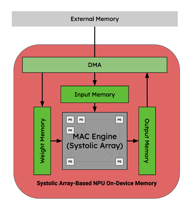
Figure 8. Memory hierarchy for a MAC acceleration systolic array NPU. Image by Author.
In the context of an ASIC’s memory hierarchy, operator fusion is possible if the intermediate tensors can continuously flow through the systolic array and on-chip processing elements without needing to communicate back to the host’s shared memory.
The most performant NPU’s are designed with operator fusion in mind for a limited set of permutations of operators. Since they are hard-wired and therefore cannot be programmed, they cannot handle memory reshaping or reorganization or even fuse some activation functions that aren’t handled by their coupled hardware blocks. To perform these operations, the programs must write back out to some shared memory: either on device or shared memory on the SoC.
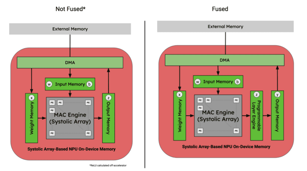
Figure 9. Tensor locations for 3x3 Conv., Bias Add, and ReLU activation function sequence of graph operators in an NPU memory hierarchy. Image by Author.
Their lack of programmability and sensitivity to some model architectures, like the increasingly popular transformers, make them inaccessible to many AI applications. Shameless plug: if you’re interested in learning more about this subject, check out our recent blog post on this topic.
For these reasons, custom NPU accelerators do not satisfy the compute generality and memory organization requirements for broadly-applicable operator fusion.
GPNPUs, like the Quadric Chimera QB16 processor, are also purpose-built processor architectures and, therefore, the way they accelerate AI varies; however, most use distributed compute elements in a mesh network for parallelization of compute and more efficient memory management.
GPNPUs strike a middle ground between NPUs and GPUs by being capable of both AI application-specific and generally programmable. Using thoughtful hardware-software co-design, they’re able to reduce the amount of hardware resources consumed while also being fully programmable.
The Chimera family of GPNPUs are fully C++ programmable processor cores containing a networked mesh of Processing Elements (PEs) within the context of a single-issue, in-order processor pipeline. Each PE has its own local register memory (LRM) and collectively are capable of running scalar, vector, and matrix operations in parallel. They’re mesh-connected thus are capable of sharing intermediate tensor data directly with neighboring PEs without writing to shared L2 memory.
Figure 10. Memory hierarchy for a Quadric GPNPU. Image by Author.
In the context of a GPNPU's memory hierarchy, two successive operations are considered to be fused if the intermediate tensor(s) between those two operations do not leave the distributed LRM, the memory block within each PE.
The difference between the PEs in a systolic array and the array of PEs in the GPNPU is that the PEs are collectively programmed to operate in parallel using the same instruction stream. Since the dataflow of most DNN operators can be statically defined using access patterns, simple APIs can be written to describe the distribution and flow of the data through the array of PEs. This greatly simplifies the developer experience because complex algorithms can be written without needing to explicitly program every internal DMA transfer. In the instance of Quadric’s Chimera processor, the Chimera Compute Library (CCL) provides all of those higher-level APIs to abstract the data movement such that the programmer does not need to explicitly gain deep knowledge of the two-level DMA within the architecture.
For these reasons, GPNPUs strike a balance between thoughtfully designed hardware for AI compute with the programmability and flexibility of a general-parallel compute platform like a GPU. GPNPUs satisfy the general compute and the memory organization requirements for operator fusion and are only limited occasionally by the memory availability requirement.
Let’s take a look at a similar practical example of operator fusion performed by a GPNPU and its compiler, the Chimera Graph Compiler (CGC).
Here’s a visual diagram of a MobileNetV2 network before and after operator fusion performed by Quadric’s Chimera™ Graph Compiler (CGC) in the style of NVIDIA’s diagram from Figure 2:
Figure 11. A MobileNetV2 module network before and after layer operator fusion performed by Quadric’s Chimera™ Graph Compiler (CGC).
In the example above, operator fusion performed by CGC was able to reduce the number of layers from 17 to 1. This feat is even more impressive when you consider the sequence of layers that were fused.
The fused layer produced by CGC contains four convolutional operators with varying number of channels and filter sizes. Since the GPNPU uses a networked mesh of PEs, data can be shared by neighboring PEs without writing back out to shared L2 memory. These data movements are an order of magnitude faster than writing out to L2 memory and allow data to “flow” through the PEs similar to how a systolic array computes MAC operations, but in a programmable way.
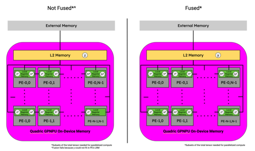
Figure 12. Tensor locations for 3x3 Conv., Bias Add, and ReLU activation function sequence of graph operators in an Quadric Chimera GPNPU memory hierarchy. Image by Author.
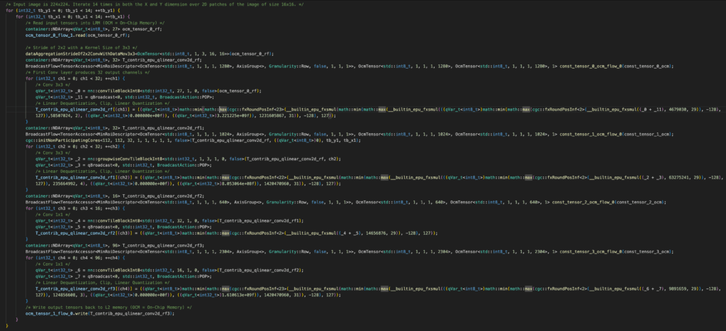
Since the PEs are collectively programmed with a single instruction stream, the APIs available to represent these operators are remarkably simple which can result in very short, but performant code. Below is the auto-generated C++ code-snippet for the MobileNetV2 operators from Figure 10 generated by Quadric’s CGC. Without comments, which have been added, it is 37 lines of code for all 17 operators:
The total size of the intermediate tensors that were fused in this code snippet and therefore not moved between LRM and L2 memory was 6,623.2 KB or ~6.6 MB. For context, the input data passed into the first layer of this block was 150.5 KB and the intermediate tensor data that was finally moved out to L2 memory was 1.2 MB. By aggressively leveraging operator fusion, CGC was able to reduce the total memory movement overhead of this section of the MobileNetV2 kernel by 83%.
For high-performance edge applications that are optimizing performance for TOPS/W, these data movement savings translate directly to power savings. Below in Figure 13 is a table of the relative costs associated with moving a 32b data element from the ALU/MAC engine register file memory on a Chimera GPNPU to each of the other levels of memory:
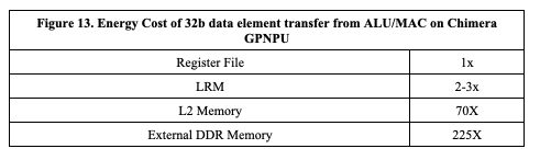
By performing operator fusion and not moving those 6.6 MB of intermediate tensor data, an application developer can expect a ~185x reduction in power consumption.
If you’re a hardware designer looking to enable high-performance, lower power AI applications for your developers and are interested in the potential performance benefits that Quadric’s Chimera Graph Compiler (CGC) can provide, consider signing up for a Quadric DevStudio account to learn more.