Nano, Perform, Ultra, Multi Chimera Processors
Chimera GPNPU Processor IP


Chimera GPNPU Processor IP 

Scale from 1 to 840 TOPs
Serves all market segments
ASIL-ready for automotive applications

Accelerator Level Performance + Processor Flexibility

Designed from the ground up to address the constantly evolving AI inference deployment challenges facing system on chip (SoC) developers, Quadric's Chimera(TM) general purpose neural processor (GPNPU) family has a simple yet powerful architecture with demonstrated improved matrix-computation performance over the traditional approach. Its crucial differentiation is its ability to execute diverse workloads with great flexibility all in a single processor.

The Chimera GPNPU family provides a unified processor architecture that handles matrix, vector and scalar (control) code in one execution pipeline. In competing NPU alternatives AI workloads are traditionally by a combination of NPU "accelerator" paired with one or both of a legacy DSP or realtime CPU, requiring splitting AI/ML graph execution and tuning performance across two or three heterogenous cores. The Chimera GPNPU is a single software-controlled core, allowing for simple expression of complex parallel workloads.

The Chimera GPNPU is entirely driven by code, empowering developers to continuously optimize the performance of their models and algorithms throughout the device’s lifecycle. That's why it's ideal to run classic backbone networks, todays' newest Transformers and Large Language Models, and whatever new networks are invented tomorrow.
Chimera GPNPU Block Diagram

Modern System-on-Chip (SoC) architectures deploy complex algorithms that mix traditional C++ based code with newly emerging and fast-changing machine learning (ML) - or "AI" -  inference code. This combination of graph code commingled with C++ code is found in numerous chip subsystems, most prominently in vision and imaging subsystems, radar and lidar processing, communications baseband subsystems, and a variety of other data-rich processing pipelines. Only Quadric’s Chimera GPNPU architecture can deliver high AI/ML inference performance and run complex, data-parallel C++ code on the same fully programmable processor. 

Compared to other inference architectures that force the software developer to artificially partition an algorithm solution between two or three different kinds of processors, Quadric’s Chimera processors deliver a massive uplift in software developer productivity while also providing current-day graph processing efficiency coupled with long-term future-proof flexibility.

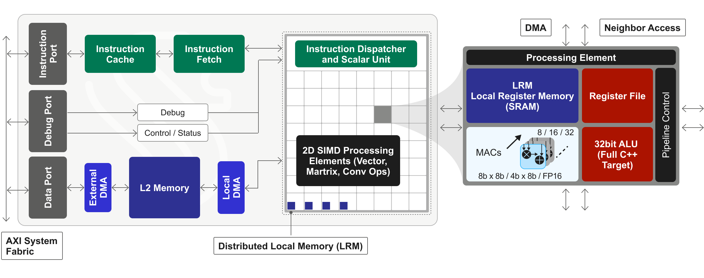
Quadric’s Chimera GPNPUs are licensable processor IP cores delivered in synthesizable source RTL form. Blending the best attributes of both neural processing units (NPUs) and digital signal processors (DSPs), Chimera GPNPUs are aimed at inference applications in a variety of high-volume end applications including mobile devices, digital home applications, automotive and network edge compute systems.

Benefits of Chimera GPNPU Processors

System Simplicity

Quadric’s solution enables hardware developers to instantiate a single core that can handle an entire AI/ML workload plus the typical digital signal processor functions and signal conditioning workloads often intermixed with inference functions. Dealing with a single core drastically simplifies hardware integration and eases performance optimization. System design tasks such as profiling memory usage and estimating system power consumption are greatly simplified.

Programming Simplicity

Quadric’s Chimera GPNPU architecture dramatically simplifies software development since matrix, vector, and control code can all be handled in a single code stream. Graph code from the common training toolsets (Tensorflow, Pytorch, ONNX formats) is compiled by the Quadric SDK and can be merged with signal processing code written in C++, all compiled into a single code stream running on a single processor core.

Quadric’s SDK meets the demands of both hardware and software developers, who no longer need to master multiple toolsets from multiple vendors. The entire subsystem can be debugged in a single debug console. This can dramatically reduce code development time and ease performance optimization.

This new programming paradigm also benefits the end users of the SoCs since they will have access to program all the GPNPU resources.

Future Proof Flexibility

A Chimera GPNPU can run any AI/ML graph that can be captured in ONNX, and anything written in C++. This is incredibly powerful since SoC developers can quickly write code to implement new neural network operators and libraries long after the SoC has been taped out. This eliminates fear of the unknown and dramatically increases a chip’s useful life.

This flexibility is extended to the end users of the SoCs. They can continuously add new features to the end products, giving them a competitive edge.

Replacing a legacy heterogenous AI subsystem comprised of separate NPU, DSP, and realtime CPU cores with one GPNPU has obvious advantages. By allowing vector, matrix, and control code to be handled in a single code stream, the development and debug process is greatly simplified while the ability to add new algorithms efficiently is greatly enhanced.

As ML models continue to evolve and inferencing becomes prevalent in even more applications, the payoff from this unified architecture helps future-proof chip design cycles.

The Chimera GPNPU Family 

The Chimera QC processor family spans a wide range of performance requirements. As a fully synthesizable processor, you can implement a Chimera IP core in any process technology, from older nodes to the most advanced technologies.  From the single-core QC Nano all the way to 8-way QC-Multi clusters, there is a Chimera processor that meets your performance goals. Talk to us about which processor you need for your design!

Key architectural features of Chimera cores 

• Hybrid Von Neuman + 2D SIMD matrix architecture
• 64b Instruction word, single instruction issue per clock
• 7-stage, in-order pipeline
• Scalar / vector / matrix instructions modelessly intermixed with granular predication
• Deterministic, non-speculative execution delivers predictable performance levels
• Configurable AXI Interfaces to system memory (independent data and instruction access)
• Configurable Instruction cache (64/128/256K)
• Distributed tightly coupled local register memories (LRM) with data broadcast networks within the matrix array allows overlapped compute and data movement to maximize performance
• Local L2 data memory (multi-bank, configurable 1MB to 16MB) minimizes off-chip DDR access, lowering power dissipation
• Optimized for INT8 machine learning inference (with optional FP16 floating point MAC support, and A8W4 MAC option) plus 32b ALU DSP ops for full C++ compiler support
• Compiler-driven, fine-grained clock gating delivers power savings

Memory Optimization = Power Minimization 

Machine Learning inference is a data & memory movement optimization problem, not a compute efficiency problem.

• Application code today benefits from two levels of compiler optimization of memory hierarchy
• Future iterations of the Chimera SDK will continue to add compiler optimization enhancements in both CGC and LLVM
Tremendous power saving are a direct result of consolidating all of the processing of the NPU, the DSP, and the realtime CPU into one GPNPU. 
ML / AI inference solutions are most often performance- and power-dissipation-limited by memory system bandwidth utilization. With most state-of-the-art AI models having millions or billions of parameters, fitting an entire model into on-chip memory within an advanced System-on-a-Chip (SoC) is generally not possible. Therefore, smart management of available on-chip data storage of both weights and activations is a prerequisite to achieving high efficiency. To further complicate the design of SoCs the rate of change of AI models – both operator types and model topologies – far outpaces the design and deployment lifecycles of modern SoC designs. System architects must pick IP today to run models of unknown complexity in the coming years.

Many second-generation NPU accelerators in systems today are hardwired finite state machines (FSMs) that offload several performance intensive building-block AI operators such as convolution and pooling. These FSM solutions deliver high efficiency only if the ultimate network to be run on the SoC does not waver from the limited scope of the operator parameters that have been hard-coded into the silicon. This hard-coded behavior extends to the supported memory management strategies deployed for those FSM accelerators. A FSM solution does not allow for future fine-tuning of memory management strategies as network workloads evolve. The Chimera processor family solves this limitation by being fully programmable and powered by compiler-driven DMA management.

A SoC design with a Chimera GPNPU has four levels of data storage. Off-chip DDR offers a vast lake of storage for even the largest new AI models. But accessing DDR is expensive both in terms of power dissipation and cycle count. Therefore, the Chimera GPNPU contains a configurable private buffer SRAM on chip - the L2 memory – which is managed by compiler-driven code. L2 size is determined by the SoC architect at chip design time and can range from 1 MB to 16 MB. L2MEM holds data that is temporally beneficial in speeding up algorithm execution, such as model weights and activations for neural networks and a variety of data and coefficients for DSP algorithms. The partitioning of the usage of L2MEM is software and compiler driven, offering long-term flexibility to adapt to changing inference workloads.

Rich DSP and Matrix Instruction Set 

The Chimera instruction set implements a rich set of operations covering the breadth of control, DSP and tensor graph processing. The base Chimera processing element (PE) is optimized for 8-bit integer inference operations with a configurable hardware option to also include 16bit Floating Point (FP16) MAC hardware. In addition to the convolution-focused multiply-accumulate hardware, a full set of math functions is available in each ALU to support all forms of complex DSP operations:

• 32-bit Integer MUL / ADD / SUB / Compare
• 32-bit Integer DIV (iterative execution)
• 32-bit Cordic function unit (Sine, Cosine, Rect. to Polar / Polar to Rect., ArcX functions)
• Logarithmic and Exp functions

A set of math function libraries harnessing these special function instructions accompanies the Chimera SDK, covering an array of common signal processing routines including cordic, linear algebra, filtering and image processing functions.

GPNPU -vs- NPU

NPU Accelerators

NPUs – neural processing units – are a type of hardware block used in semiconductor chip design to accelerate the performance of machine learning / artificial intelligence workloads. NPUs are generally referred to as accelerators or offload engines and are paired with pre-existing legacy programmable processors such as CPUs, GPUs and DSPs.

The NPU concept first was conceived circa 2015 as silicon designers realized that emerging new AI/ML algorithms would not run at sufficiently high speeds on legacy CPU, DSP or GPU processors, hence the idea of “offloading” portions of the machine learning graph onto an accelerator.

The concept is simple: identify the most performance intensive elements of the AI/ML workload - the matrix multiplication common in convolutional neural networks - and carve that out of the graph to run on a specialized hardware engine, leaving the remainder of the algorithm to run on the original CPU or DSP.

Virtually all commercially licensable NPUs follow this approach, often sold alongside the original legacy processor offered by the IP vendor. Under this concept, both the legacy CPU or DSP host and the NPU are dedicated in tandem to running the AI/ML workloads. The NPU is a fixed-function block with a set “vocabulary” of AI functions – or Operators – that it can execute, and the CPU/DSP carries the rest of the workload. If newer algorithms are invented with different operators, more of that future workload defaults to running on the legacy CPU/DSP, potentially negatively impacting the overall throughput performance of the device.

GPNPU Processors

GPNPUs – general purpose neural processing units – are a type of fully C++ programmable processor IP used in semiconductor chip design. GPNPUs run entire AI/ML workloads fully self-contained without the need for a companion CPU, DSP or GPU.

GPNPUs blend the high matrix performance of an NPU with the flexibility and programmability of traditional processors. GPNPUs – such as Quadric’s Chimera GPNPU - are future-proof because new operators can be easily written as new C++ kernels running at high-speed on the GPNPU itself. And because GPNPUs are code-driven, a compilation toolchain automates the targeting of new algorithms to the GPNPU with hundreds of different AI models compiled automatically to the platform.

© Copyright 2025  Quadric    All Rights Reserved     Privacy Policy

linkedin facebook pinterest youtube rss twitter instagram facebook-blank rss-blank linkedin-blank pinterest youtube twitter instagram