Not just a little slow down. A massive failure!
Conventional AI/ML inference silicon designs employ a dedicated, hardwired matrix engine – typically called an “NPU” – paired with a legacy programmable processor – either a CPU, or DSP, or GPU. You can see this type of solution from all of the legacy processor IP licensing companies as they try to reposition their cash-cow processor franchises for the new world of AI/ML inference. Arm offers an accelerator coupled to their ubiquitous CPUs. Ceva offers an NPU coupled with their legacy DSPs. Cadence’s Tensilica team offers an accelerator paired with a variety of DSP processors. There are several others, all promoting similar concepts.
The common theory behind these two-core (or even three core) architectures is that most of the matrix-heavy machine learning workload runs on the dedicated accelerator for maximum efficiency and the programmable core is there as the backup engine – commonly known as a Fallback core – for running new ML operators as the state of the art evolves.
As Cadence boldly and loudly proclaims in a recent blog : “The AI hardware accelerator will provide the best speed and energy efficiency, as the implementation is all done in hardware. However, because it is implemented in fixed-function RTL (register transfer level) hardware, the functionality and architecture cannot be changed once designed into the chip and will not provide any future-proofing.” Cadence calls out NPUs – including their own! - as rigid and inflexible, then extols the virtues of their DSP as the best of the options for Fallback. But as we explain in detail below, being the best at Fallback is sorta like being the last part of the Titanic to sink: you are going to fail spectacularly, but you might buy yourself a few extra fleeting moments to rue your choice as the ship sinks.
In previous blogs, we’ve highlighted the conceptual failings of the Fallback concept. Let’s now drill deeper into an actual example to show just how dreadfully awful the Fallback concept is in real life!
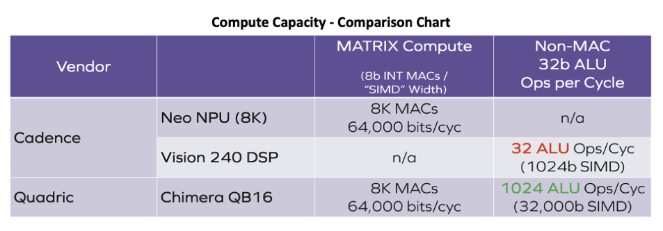
Let’s compare the raw computational capacity of the conventional architecture concept using Cadence’s products as an example versus that of Quadric’s dramatically higher performance Chimera GPNPU. Both the Cadence solution chosen for this comparison and the Quadric solution have 16 TOPs of raw machine learning horsepower – 8K multiply-accumulate units each, clocked at 1 GHz. Assuming both companies employ competent design teams you would be right to assume that both solutions deliver similar levels of performance on the key building block of neural networks – the convolution operation.
But when you compare the general-purpose compute ability of both solutions, the differences are stark. Quadric’s solution has 1024 individual 32bit ALUs yielding an aggregate of 32,000 bits of ALU parallelism, compared to only 1024 bits for the Cadence product. That means any ML function that needs to “fall back” to the DSP in the Cadence solution runs 32 times slower than on the Quadric solution. Other processor vendor NPU solutions are even worse than that! Cadence’s 1024-bit DSP is twice as powerful as simpler 512-bit DSPs or four times as powerful as vector extensions to CPUs that only deliver 256-bit SIMD parallelism. Those other products are 64X or 128X slower than Quadric!
ConvNext – A Specific, Current Day Example
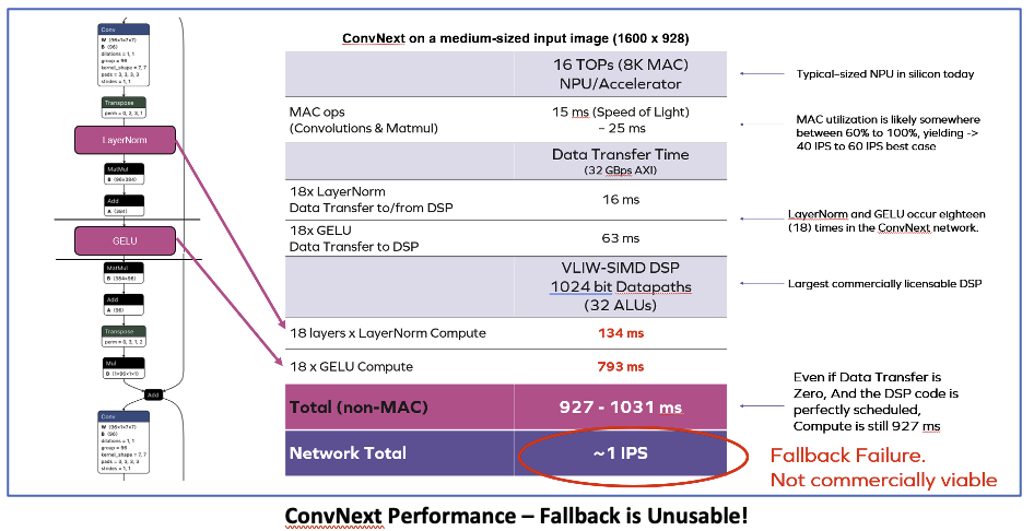
One of the more recent new ML networks is ConvNext, boasting top-1 accuracy levels of as much as 87.8% - nearly 10 full percentage points higher than the Resnet architectures of just a few years ago. Two key layers in the ConvNext family of networks that typically are not present in fixed-function NPUs are the LayerNorm normalization function and the GeLU activation used in place of the previously more common ReLU activation. In the conventional architectures promoted by other IP vendors, the GeLU and LayerNorm operations would run on the FallBack DSP, not the accelerator. The result – shown in the calculations in the illustration below – are shocking!
Fallback Fails – Spectacularly
Our analysis of ConvNext on an NPU+DSP architecture suggests a throughput of less than 1 inference per second. Note that these numbers for the fallback solution assume perfect 100% utilization of all the available ALUs in an extremely wide 1024-bit VLIW DSP. Reality would undoubtably be below the speed-of-light 100% mark, and the FPS would suffer even more. In short, Fallback is unusable. Far from being a futureproof safety net, the DSP or CPU fallback mechanism is a death-trap for your SoC.
Is ConvNext an Outlier?
A skeptic might be thinking: “yeah, but Quadric probably picked an extreme outlier for that illustration. I’m sure there are other networks where Fallback works perfectly OK!”. Actually, ConvNext is not an outlier. It only has two layer types requiring fallback. The extreme outlier is provided to us by none other than Cadence in the previously mentioned blog post. Cadence wrote about the SWIN (shifted window) Transformer:
“When a SWIN network is executed on an AI computational block that includes an AI hardware accelerator designed for an older CNN architecture, only ~23% of the workload might run on the AI hardware accelerator’s fixed architecture. In this one instance, the SWIN network requires ~77% of the workload to be executed on a programmable device.”
Per Cadence’s own analysis: 77% of the entire SWIN network would need to run on the Fallback legacy processor. At that rate, why even bother to have an NPU taking up area on the die – just run the entire network – very, very slowly – on a bank of DSPs. Or, throw away your chip design and start over again - if you can convince management to give you the $250M budget for a new tapeout in an advanced node!
Programmable, General Purpose NPUs (GPNPU)
There is a new architectural alternative to fallback – the Chimera GPNPU from Quadric. By merging the best attributes of dataflow array accelerators with full programmability (see last month’s blog for details) Quadric delivers high ML performance while maintaining endless programmability. The basic Chimera architecture pairs a block of multiply-accumulate (MAC) units with a full-function 32bit ALU and a small local memory. This MAC-ALU-memory building block – called a processing element (PE) - is then tiled into a matrix of 64, 256 or 1024 PEs to form a family of GPNPUs offering from 1 TOP to 16 TOPs each, and multicore configurations reaching hundreds of TOPs. Part systolic array and part DSP, the Chimera GPNPU delivers what Fallback fails to deliver – the promise of efficiency and complete futureproofing. See more at quadric.io.
© Copyright 2025 Quadric All Rights Reserved Privacy Policy