The term “model zoo” first gained prominence in the world of AI / machine learning beginning in the 2016-2017 timeframe. Originally used to describe open-source public repositories of working AI models – the most prominent of which today is Hugging Face – the term has since been adopted by nearly all vendors of AI chips and licensable neural processors (NPUs) to describe the set of working models that have been ported to those vendors’ specific platforms.
Why Vendor-Specific Zoos In the First Place?
Understanding model zoos starts with understanding the origin of the “animals” in the zoos. Data scientists create new AI models by inventing and training the models. That training process is dominated almost entirely by researchers using Nvidia GPUs as the training hardware and training software frameworks such as PyTorch and Tensorflow. Almost 100% of such models are created and published using floating point data types (FP32). FP32 delivers the highest possible accuracy and is a native data type for NVDA GPUs.
While FP32 is great for ease of training, it is not energy efficient as a data representation for real-world AI inference. NPUs – neural processors – in edge devices and embedded systems typically perform most AI inference computations using 8-bit Integer data formats (INT8), and some systems are pushing to even smaller formats (INT4, others). The advantages of INT8 versus FP32 are stark – 10X to 20X lower energy consumption per unit of computation, plus dramatic model size reduction arising from converting model weights from 32bits per element to only 8 or fewer bits per element. Take, for example, the idea of running 8 billion parameter Large Large Model (LLM) on a phone or laptop: executing the model in the original FP32 format would entail needing 4 x 8 = 32 GBytes of DRAM on your phone just to hold the model weights, and to stream that entire model from DDR into the phone applications processor SoC repeatedly for each token generated. 32GB of DDR is cost and power prohibitive on a phone. Compressing the model weights to 8bit Integer or 4bit integer formats makes it practical to execute such a model on your phone. As a result, every commercially available NPU uses one or more data types that are dramatically smaller than FP32, with the majority of NPUs using INT8 as the basic building block.
Sadly, converting a model – a process known as Quantization – is neither pushbutton nor uniform. Merely blindly converting every layer and every model weight from the high precision of floating point to the more granular INT8 format often unacceptably reduces model accuracy. Some operators need to be preserved in higher-precision data formats. That’s where the conversion process gets tricky. Each NPU and each SoC architecture has different compute resources with different data types – INT4, INT8, INT16, FP16, FX32, FP32, and others. Picking and choosing which model layers to treat with high data precision and then choosing an available data format in the target AI chip takes engineering effort and powerful analytical tooling.
The net result is that because this “porting” of published models to a specific platform takes effort, the various AI chip and NPU vendors publish collections of pre-ported models that are known to work on their platforms with acceptable accuracy loss compared to the original model.
Zoo Population Size – a Proxy for Ease of Use?
The process of porting a new AI model to a given NPU accelerator is not uniformly speedy or straightforward. The effort involves both a data science component (choosing the optimal quantization strategies and data precisions) as well as an embedded software performance tuning component. That performance tuning is simple and easy if the target platform has an all-in-one, general purpose NPU such as the Quadric Chimera GPNPU processor. But if the target silicon employs a heterogeneous architecture with a combination of CPU plus DSP plus hard-wired NPU accelerator then many AI model graph layers could be executed on two or three different compute engines, and the software engineer has to select which layers run on the different resources and tune the use of memory accordingly to achieve acceptable inferences per second performance.
Is therefore a reasonable conclusion to judge that the size of the available model zoo – i.e. the number of animals in the zoo – is a reflection of two main factors: [1] the ease of use of the vendor-specific porting tools; and [2] the relative popularity of the platform – i.e. how many engineers are working to port and publish new models in that zoo.
Mine is Bigger than Yours!
Let us take a look at several public zoos / code repositories to judge the Productivity * Popularity metric. The following table shows data from a snapshot taken from public model repos as of September 2025. It also shows the approximate funding levels (data from Crunchbase) or employee headcount size for the vendor.
| NPU Vendor | Funding Raised / Employee Headcount | NPU Models in the Zoo – September 2025 |
| Well known RISC-V NPU proponent | Funding > $1B Headcount > 1000 | 49 models |
| Market Leading CPU & NPU Licensor | Market Capitalization > $140B Headcount > 8000 | 43 models |
| Publicly listed Asian GPU/NPU licensor and ASIC provider | Market Capitalization > $15B | 72 models |
| Quadric | Funding (thru mid-2025): $43M Headcount < 100 | 352 Model examples 110 models added in 2025 |
Our attorneys recommended that we not call out those competitors by name and to not include clickable hyperlinks to their underpopulated zoos. But we think you can do your own homework on that topic.

Simply Better Architecture and Tools!
The comparison is shocking. Tiny – but rapidly growing – Quadric is running laps around the Other Guys in the race to populate the model zoo. It’s certainly not because we spend more money and have more engineers porting models. The reason for the disparity is simply our vastly superior underlying architecture and accompanying toolchain. Quadric’s Chimera GPNPU natively executes every layer of every AI model without needing to partition the model and Fallback to a legacy CPU or DSP. Quadric’s Chimera Graph Compiler (CGC) automatically lowers (compiles) AI models from their native ONNX graph format into a C++ representation of the graph, which is then compiled by the LLVM C++ compiler to run end-to-end on the Chimera processor. And most critically when a new AI model cannot automatically compile – usually because of a proprietary graph structure that they want to keep private - users can rapidly write the missing functionality by themselves in common everyday C++ to complete the model port without any intervention from Quadric.
To Solve AI Compute Challenge, Choose a Purpose-Built NPU Do you want to see the Quadric model zoo for yourself? Check out the online Quadric DevStudio at studio.quadric.io to see the full list of classic models, transformers, LLMs and DSP pre- and post-processing code
In the 1986 hit comedy movie Crocodile Dundee, the title character – a rough and tumble Australian transported to the mean streets of New York City – is confronted by street thugs brandishing a switchblade knife who demand his wallet. In response he cooly smirks and pulls a knife out of his belt that is 10 times the size of the would-be assailants’ weapon and delivers the signature line of dialog of the film, “That’s not a knife. <pauses, pulls out his own much larger weapon> Now, THAT’S a knife!”
Shaking Your Head Wondering: What Does This Have To Do With Embedded AI?
Regular readers of this blog are likely familiar with the author’s penchant for obscure analogies. So you’re probably wondering “how does Crocodile Dundee relate to SoC design?” In the same way that Mick Dundee brought a much bigger knife to a knife fight, the same thing holds true if you are to believe the marketing claims of many of the would-be AI NPU licensors who highlight the wonders of their DSPs (or vector extensions to their CPUs) as the magical elixir to solve the programmability problem with matrix accelerators: the bigger the DSP the better.
AI Graphs: Matrix Ops plus “ALU” Ops
Modern AI or Machine Learning workloads are both computationally intensive (billions of calculations) as well as complex (hundreds or thousands of different operations). A full decade ago – 2015 – the ResNet family of CNNs was first published. While the workhorse ResNet50 network was far too computationally intensive to run on the existing CPUs or DSPs of the day, the highly repetitive nature of Resnets – Resnet18, for instance, consists of the same 8 operators repeated 18 times in the “backbone” of the graph – made them ideal candidates to accelerate using fixed-function matrix offload engines attached to legacy CPUs or DSPs.
But the intervening decade of rapid innovation has rendered the simple offload NPU as obsolete. Today’s leading AI training framework, Pytorch, has more than 2300 different graph operators. Modern transformer networks can have 300 or more variants of operators intertwined with each other – matrix operations followed by mathematically complex arithmetic operations (e.g. root mean square calculations, sigmoid calculations, others) followed by more matrix multiplication filtering. The common approach to implement these varied operations is to build efficient multiply-accumulate engines (MAC arrays) along side more flexible, more general-purpose arithmetic logic units (ALUs) that run the non-MAC functions.
The Size of the Knife
Legacy CPU and DSP vendors tout the added vector processing width in their newest and biggest DSPs and CPU vector extensions as the perfect “future proofing” answer for the next unexpected AI algorithm breakthrough. Countless RISC-V startups highlight their novel 512-bit or 1024-bit vector extensions to the CPU instruction set. DSP vendors have pushed VLIW machine widths from 256 bits up to 512 bits and now 1024 bits, with some even supporting as many as four simultaneous VLIW bundles operating 4 x 256 = 1024 bits in parallel. Thus, if these aspiring NPU licensing companies can magically manage to eliminate the data transfer penalties associated with physically separate NPU and DSP engines, a fact they conveniently ignore in their marketing, they claim their 1024 bit “knives” are the weapon of choice for the AI knife fight.
That’s Not a DSP. THIS is a DSP!
Is a 1024-bit DSP really the solution you want in your next chip as you fight the evolving AI battle? Or would you want a Crocodile Dundee-sized DSP solution? Quadric’s Chimera architecture is unique in crafting building blocks placing small tiles of MACs immediately adjacent to a full-fledged, programmable 32bit ALU. That building block (MACs, ALU, SRAM) is tiled in two-dimensional array fashion. The largest of our three general purpose NPU (GPNPU) processors – the Chimera QC Ultra – contains 1024 building block tiles all operating in unison executing the same instruction. That’s 1024 ALUs, each 32b wide. 32,768 bits of fully C++ programmable parallelism. Thirty-two times larger and faster than any competing AI processor offering. As Mick Dundee would say. “Now, THAT’S a DSP!”
At some point in everyone’s teenage years of schooling we were all taught in a nature or biology class about cycles of population surges and then inevitable population collapses. Whether the example was an animal, plant, insect or even bacteria, some external event triggers a rapid surge in the population of a species which leads to overpopulation and competition for resources (food, space, shelter) at which point either the surge in population exhausts the food supply, or the species itself becomes food for some other predator that decimates the local population. The cycle is consistent: external trigger, population surge, resource exhaustion, and finally a collapse back to a population level that can be sustained long term in the native habitat’s normal state of affairs.
The same cycle of Boom and Bust applies to the business enterprises that we humans create in response to economic opportunities. Cycles of production in new house construction, oil production or even trendy boba tea merchants see waves of new ventures followed by inevitable market shakeouts that thin the herd where weaker players disappear, and strong competitors survive and thrive. The semiconductor and semiconductor IP businesses are no different, as observers with long memories can no doubt recall.
IP Industry Shakeouts of the Past
For the past 25 years every time a new interface standard emerges, or a new design trend becomes mainstream, we’ve witnessed a surge of both IP suppliers and chip startups that attempt to race to market and grab a piece of the emerging pie. In the world of processor IP, we’ve seen this happen with CPUs, DSPs, GPUs and even esoteric categories such as packet processors.
Consider, for instance, the huge population of CPU and DSP architectures that existed in the year 2000. The image below shows the three public processor IP companies from late 2000 as well some of the more than 40 other companies either licensing cores or building silicon and systems with competing CPUs or DSP.
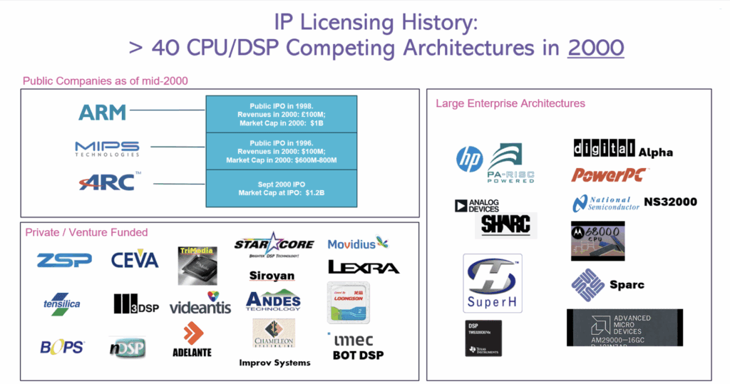
The semiconductor world did not need – and could not support – all 40 architectures. That surge of market participants occurred because it was the beginning of the age of System on Chip design. SoCs need processors and thus many processors were either born or spun out of existing tech companies. Within a few years of that Y2K peak population the number of CPU and DSP licensing companies collapsed to less than 10. Most the names and logos in that image above ceased to exist by 2005 while several of the survivors (such as Tensilica and Arc) were gobbled up by bigger companies.
Following the analogy of the natural world, it’s fair to ask what “resource scarcity” did those CPU/DSP companies run out of? Two primary ingredients ran short: investment capital and compiler talent. Investors do not have infinite patience and thus many enterprises begun during the population explosion years of 1998-2000 (which coincides with one of the biggest stock valuation bubbles of all time!) could not sustain themselves beyond 2005. And less competitive architectures that were difficult to program suffered as they struggled to hire enough compiler talent to build advanced tools to compensate for inferior architectures. The clock ran out for most of those names.
NPUs Today - We’ve Seen this Movie Before!
25 years removed from Peak CPU/DSP we are seeing the same movie being replayed with different actors in the world of NPU architectures. The external trigger: the meteoric rise of AI and the rush to embed AI horsepower in every device from your smartwatch to the giant datacenter. A tidal wave of opportunity drew a flood of investment dollars from 2018 thru 2024.
This second image captures a snapshot of just some of the competing NPU accelerator offerings – as IP and embedded in silicon - from just two years ago, when the wave of NPUs was at its peak.
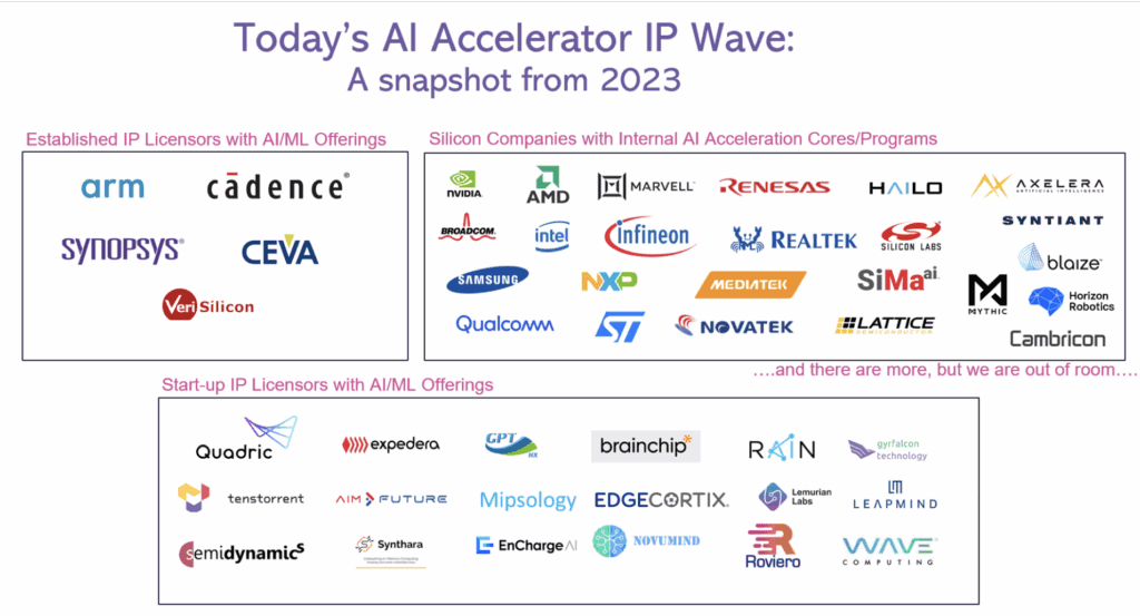
Already we’ve seen several of these names disappear as each successive rapid change in AI – such as the emergence of transformers, then LLMs – rendered wave after wave of fixed-function accelerators obsolete. Today, the same scarcities that doomed the herd of CPU startups a generation ago is now rapidly thinning the herd of AI acceleration startups in today’s market. Silicon startups are failing or being acqui-hired for their engineers (the latest: Untether). NPU licensing companies struggle to build sophisticated compilers that map ever more complex AI algorithms to unnecessarily complex architectures that bolt together legacy processors with matrix accelerators. And most ominously, venture investors are no longer willing to endlessly write big checks for round after round of frenzied investment. Instead, they demand to see market traction – either silicon volume ramps or increasing licensing success.
How Many Will Survive? The world doesn’t need, and cannot support, 50+ NPUs. Nor does the world want to see only 1 survivor - no one likes having an 800lb gorilla dominate a market. 50+ will dwindle down to 5 to 10 winners. 2025 will be an inflection point in the NPU world as the population of contenders collapses. The winners will be marked by: (1) superior software toolchains (compilers) that can handle thousands or tens of thousands of AI models; (2) tooling that empowers end users to easily program new AI models onto silicon as data scientists continue to innovate as a rapid pace; and (3) business traction that attracts the fresh capital needed to continue to invest and grow.
Five or six years ago, CPU IP providers jumped into the NPU accelerator game to try to keep their CPUs relevant with a message of “use our trusted CPU and offload those pesky, compute hungry matrix operations to an accelerator engine.” DSP IP providers did the same. As did configurable processor IP vendors. Even GPU IP licensing companies did the same thing.
The playbook for those companies was remarkably similar: (1) tweak the legacy offering instruction set a wee bit to boost AI performance slightly, and (2) offer a matrix accelerator to handle the most common one or two dozen graph operators found in the ML benchmarks of the day: Resnet, Mobilenet, VGG.
The result was a partitioned AI “subsystem” that looked remarkably similar across all the 10 or 12 leading IP company offerings: legacy core plus hardwired accelerator.
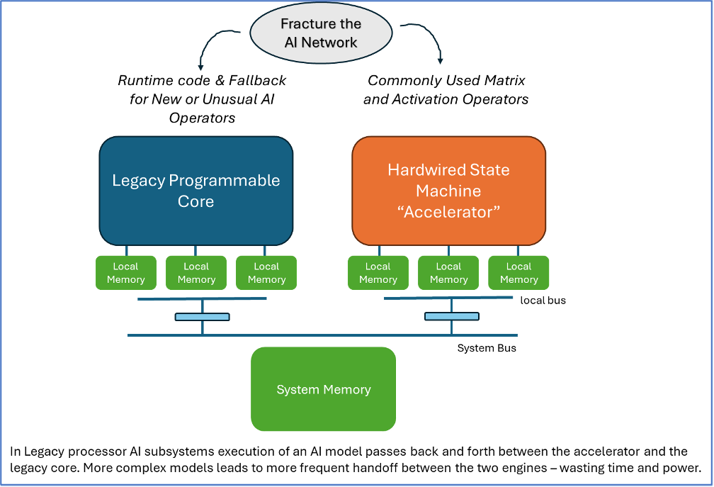
The fatal flaw in these architectures: always needing to partition the algorithm to run on two engines. As long as the number of “cuts” of the algorithm remained very small, these architectures worked very well for a few years. For a Resnet benchmark, for instance, usually only one partition is required at the very end of the inference. Resnet can run very efficiently on this legacy architecture. But along came transformers with a very different and wider set of graph operators that are needed, and suddenly the “accelerator” doesn’t accelerate much, if any, of the new models and overall performance became unusable. NPU accelerator offerings needed to change. Customers with silicon had to eat the cost – a very expensive cost – of a silicon respin.
An Easy First Step that Quickly Was Outdated
Today these IP licensing companies find themselves trapped. Trapped by their decisions five years ago to take an “easy” path towards short-term solutions. The motivations why all of the legacy IP companies took this same path has as much to do with human nature and corporate politics as it does with technical requirements.
When what was then generally referred to as “machine learning” workloads first burst onto the scene in vision processing tasks less than a decade ago, the legacy processor vendors were confronted with customers asking for flexible solutions (processors) that could run these new, fast-changing algorithms. Caught flat-footed with processors (CPU, DSP, GPU) ill-suited to these news tasks, the quickest short-term technical fix was the external matrix accelerator. The option of building a longer-term technical solution - a purpose built programmable NPU capable of handling all 2000+ graph operators found in the popular training frameworks – would take far longer to deliver and incur much more investment and technical risk.
The Not So Hidden Political Risk
But let us not ignore the human nature side of the equation faced by these legacy processor IP companies. A legacy processor company choosing a strategy of building a completely new architecture – including new toolchains/compilers – would have to explicitly declare both internally and externally that the legacy product was simply not as relevant to the modern world of AI as that legacy (CPU, DSP, GPU) IP core previously was valued. The breadwinner of the family that currently paid all the bills would need to pay the salaries of the new team of compiler engineers working on the new architecture that effectively competed against the legacy star IP. (It is a variation on the Innovator’s Dilemma problem.) And customers would have to adjust to new, mixed messages that declare “the previously universally brilliant IP core is actually only good for a subset of things – but you’re not getting a royalty discount.”
All of the legacy companies chose the same path: bolt a matrix accelerator onto the cash cow processor and declare that legacy core still reigns supreme. Three years later staring at the reality of transformers, they declared the first-generation accelerator obsolete and invented a second one that repeated the same shortcomings of the first accelerator. And now faced with the struggles of the 2nd iteration hardwired accelerator having also become obsolete in the face of continuing evolution of operators (self-attention, multiheaded self-attention, masked self-attention, and more new ones daily) they either have to double-down again and convince internal and external stakeholders that this third time the fixed-function accelerator will solve all problems forever; or admit that they need to break out of the confining walls they’ve built for themselves and instead build a truly programmable, purpose-built AI processor.
Quadric Did Something Very Different
At Quadric we do a lot of first-time introductory visits with prospective new customers. As a rapidly expanding processor IP licensing company that is starting to get noticed (even winning IP Product of the Year!) such meetings are part of the territory. Which means we hear a lot of similar sounding questions from appropriately skeptical listeners who hear our story for the very first time. The question most asked in those meetings sounds something like this:
“Chimera GPNPU sounds like the kind of breakthrough I’ve been looking for. But tell me, why is Quadric the only company building a completely new processor architecture for AI inference? It seems such an obvious benefit to tightly integrate the matrix compute with general purpose compute, instead of welding together two different engines across a bus and then partitioning the algorithms. Why don’t some of the bigger, more established IP vendors do something similar?”
The answer I always give: “They can’t, because they are trapped by their own legacies of success!”
The legacy companies might struggle to decide to try something new. But the SoC architect building a new SoC doesn’t have to wait for the legacy supplier to pivot. A truly programmable, high-performance AI solution already exists today.
The Fully Programmable Chimera Architecture
The Chimera GPNPU from Quadric runs all AI/ML graph structures. The revolutionary Chimera GPNPU processor integrates fully programmable 32bit ALUs with systolic-array style matrix engines in a fine-grained architecture. Up to 1024 ALUs in a single core, with only one instruction fetch and one AXI data port. That’s over 32,000 bits of parallel, fully-programmable performance.
The flexibility of a processor with the efficiency of a matrix accelerator. Scalable up to 864 TOPS for bleeding-edge applications, Chimera GPNPUs have matched and balanced compute throughput for both MAC and ALU operations so no matter what type of network you choose to run they all run fast, low-power and highly parallel. When a new AI breakthrough comes along in five years, the Chimera processor of today will run it – no hardware changes, just application SW code.
Change is constant in the AI world. Several new and complicated transformer models have emerged in the past 18 to 24 months as new “must have” networks in advanced automotive use cases. The problem is that these novel architectures often introduce new network operators or novel ways of combining tensors – often from different types of sensors – in ways to enhance detection and recognition of objects in L3 / L4 / L5 ADAS and autonomous driving software stacks.
Here are just a few examples: Deformable Attention Transformer (DAT) and DAT++; SegFormer; Detection Transformer (DETR); and Bird’s Eye View Depth Estimation – BEVdepth. These new functions and operations in these advanced networks can pose extreme porting challenges for SoC programmers trying to run the models on existing NPU accelerators!
The Challenge of Fixed-Function Accelerators
If the car platform or SoC team is lucky, a new graph operator in a novel AI network can be supported by the existing hardwired, less-than-fully programmable NPU. This often is NOT the case, and then the operation needs to fallback to run on the slow companion CPU or DSP – which usually means the performance is so slow as to be unviable.
But what if the breakthrough function is so new, so novel, that it doesn’t exist in the common graph manipulation tools? What if the new function is not a graph operator at all?
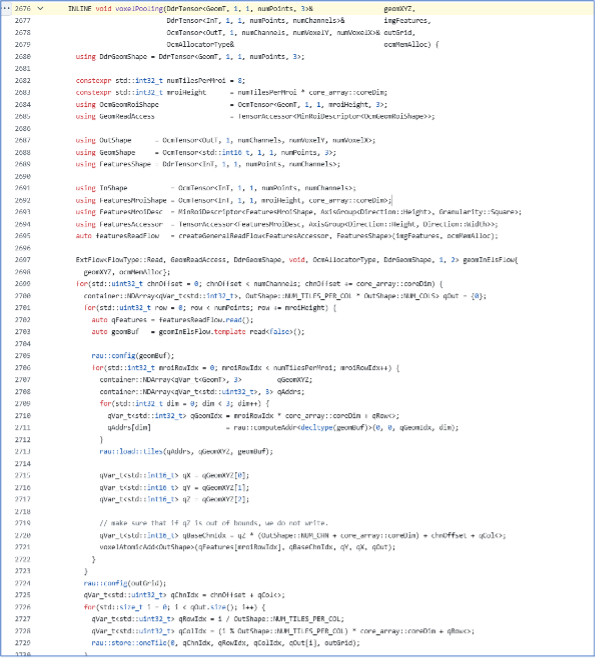
A Look at a Custom CUDA Function - Voxel Pooling
One such totally new function is the Voxel Pooling operation found in the BEVdepth network. (Available on Megvii’s public Github repo.) A trusty AI search engine describes Voxel Pooling as: “a technique where 3D point cloud data from multiple camera views is aggregated into a bird's-eye view (BEV) feature map by dividing the space into voxels (3D grid cells) and combining the features of points falling within each voxel, essentially creating a unified representation of the scene in a 2D grid format, which is then used for further processing like object detection.” Sounds complicated. In fact, in the specific case of BEVdepth, the complex voxel pooling function is written as a custom CUDA function, because it has no equivalent built-in graph operator in PyTorch today, and certainly not in the commonly used interchange formats used by NPU vendor toolchains: ONNX and TFlite.
So how does the algorithm porting team port Voxel Pooling onto an embedded NPU if the function is not represented in the graph interchange format supported by the NPU vendor’s graph compiler toolchain? With other NPUs, the team is stuck – there’s simply no way to get that important new function ported quickly to the NPU, and very likely it can never be ported. BEVdepth might simply not be able to run on the platform at all.
Only One Embedded AI Processor that Can Run This
There is only one embedded AI processor on the market that does support novel, custom operator functions in a C++ language. Quadric’s Chimera GPNPU – general purpose NPU – is programmed in C++. The advanced Chimera Graph Compiler (CGC) ingests networks in the ONNX format – from PyTorch, Tensorflow, or any other training framework. CGC then converts the entire network into optimized C++ for later compilation by the LLVM compiler.
But for functions like Voxel Pooling that are written in pure CUDA no direct compilation is possible – not with our CGC graph compiler – nor any other NPU graph compiler. The solution for Voxel Pooling is to capture the function in a custom C++ representation using our CCL dialect of C++, which is exactly how BEVdepth Voxel Pooling was written in CUDA for the Nvidia platform.
A skilled programmer who can already write CUDA code should have no trouble writing Voxel Pooling or other similar functions. The entire Voxel Pooling kernel is some sixty lines of CCL code (including comments!), shown here:
Quickly Stitch It Back Together
The C++ shown above is quickly stitched together with the auto-generated C++ output by the CGC graph compiler, and the full network is now ported completely on the Chimera GPNPU – none of the graph needs to run on any other IP block – no CPU load, no companion DSP needed.
The Chimera GPNPU is Faster Than an Nvidia GPU
You are probably already thinking: “OK, fine, you can run Voxel Pooling. But at what speed? If its not fast, it’s not useful!” Fear not! The implementation of Voxel Pooling on the Chimera GPNPU is actually faster than the original CUDA code running on a 450 Watt Nvidia RTX3090 board (with GT102 GPU chip). The Chimera GPNPU core – burning just a couple of Watts of power dissipation (your mileage will vary depending on the process node and clock frequency, and choices of off-chip memory interface) outperforms the 450W full chip GPU by a factor of 2X.
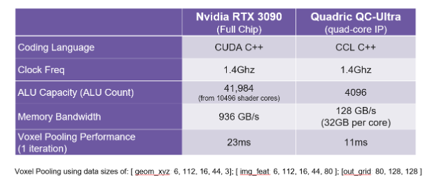
You might also wonder, “How can that be true?” Here’s why. GPUs – such as the RTX3090 – are designed for ease of use in model training and drawing polygons, mostly aimed at datacenters where electricity use is not priority #1. GPUs use cache-based architectures (caches burn power!) and hardware-heavy Warp & Thread programming models. The Chimera GPNPU processor is, by contrast, designed for embedded use. Quantized models, ahead-of-time offline compilation, and DMA-based memory hierarchy all save gobs and gobs of power.
Want to know more about the implementation of Voxel Pooling on Chimera cores? We have a detailed Tutorial – including source, performance profiling and more data - for registered users of the Quadric Dev Studio.
Chimera is a Universal, High-Performance GPNPU Solution The Chimera GPNPU runs all AI/ML graph structures. And runs non-graph code – so you can run things currently captured in CUDA, C++ (for DSP functions) and even some Python! The revolutionary Chimera GPNPU processor integrates fully programmable 32bit ALUs with systolic-array style matrix engines in a fine-grained architecture. Up to 1024 ALUs in a single core, with only one instruction fetch and one AXI data port. That’s over 32,000 bits of parallel, fully programmable performance. Scalable up to 864 TOPs for bleeding-edge ADAS applications, Chimera GPNPUs have matched and balanced compute throughput for both MAC and ALU operations so no matter what type of network you choose to run they all run fast, low-power and highly parallel.
What’s a VLM? Vision Language Models are a rapidly emerging class of multimodal AI models that’s becoming much more important in the automotive world for the ADAS sector. VLMs are built from a combination of a large language model (LLM) and a vision encoder, giving the LLM the ability to “see.” This new technology is really shaking up the industry.
The introduction of DeepSeek in January 2025 captured headlines in every newspaper and online inviting comparisons to the Sputnik moment of 1957. But rapid change is also happening in many areas that are hidden from the general public – and VLMs are a great example of this rapid change.
Why are VLMs so Important?
The big thing with VLMs is their ability to describe in text form – hence understandable by the human driver - what a camera or radar sensor “sees” in a driver assistance system in a car. A properly calibrated system deploying VLMs and multiple cameras could therefore be designed to generate verbal warnings to the driver, such as “A pedestrian is about to enter the crosswalk from the left curb 250 meters down the road.” Or such scene descriptions from multiple sensors over several seconds of data analysis could be fed into other AI models which make decisions to automatically control an autonomous vehicle.
How New are VLMs?
VLMs are very, very new. A Github repo that surveys and tracks automotive VLM evolution (https://github.com/ge25nab/Awesome-VLM-AD-ITS) lists over 50 technical papers from arxiv.org describing VLMs in the autonomous driving space, with 95% of the listing coming from 2023 and 2024. In our business at Quadric – where we have significant customer traction in the AD / ADAS segment – vision language models were rarely mentioned 18 months ago by customers doing IP benchmark comparisons. By 2024 LLMs in cars become a “thing” and designers of automotive silicon began asking for LLM performance benchmarks. Now, barely 12 months later, the VLM is starting to emerge as a possible benchmark litmus test for AI acceleration engines for auto SoCs.
What’s the Challenge of Designing for VLMs on Top of All the Other Models?
Imagine the head spinning changes faced by the designers of hardware “accelerators” over the past four years. In 2020-2022, the state-of-the-art benchmarks that everyone tried to implement were CNNs (convolutional neural networks). By 2023 the industry had pivoted to Transformers – such as SWIN transformer (shifted window transformer) as the Must Have solution. Then last year it was newer transformers – such as BEVformer (birds eye view transformer) or BEVdepth – plus LLMs such as Llama2 and Llama3. And today, pile on VLMs in addition to needing to run all the CNNs and vision Transformers and LLMs. So many networks, so many machine learning operators in the graphs! And, in some cases such as the BEV networks, functions so new that the frameworks and standards (PyTorch, ONNX) don’t support them and hence the functions are implemented purely in CUDA code.
Run all networks. Run all operators. Run C++ code, such as CUDA ops? No hardwired accelerator can do all that. And running on a legacy DSP or legacy CPU won’t yield sufficient performance. Is there an alternative?
Why You Need a Fully Programmable, Universal, High-Performance GPNPU Solution
Yes, there is a solution that has been shown to run all those innovative AI workloads, and run them at high-speed! The revolutionary Chimera GPNPU processor integrates fully programmable 32bit ALUs with systolic-array style matrix engines. Up to 1024 ALUs in a single core, with only one instruction fetch and one AXI data port. That’s over 32,000 bits of parallel, fully-programmable performance. Scalable up to 864 TOPs for bleeding-edge ADAS applications, Chimera GPNPUs have matched and balanced compute throughput for both MAC and ALU operations so no matter what type of network you choose to run - or whatever style of network gets invented in 2026 - they all run fast, low-power and highly parallel.
A common approach in the industry to building an on-device machine learning inference accelerator has relied on the simple idea of building an array of high-performance multiply-accumulate circuits – a MAC accelerator. This accelerator was paired with a highly programmable core to run other, less commonly used layers in machine learning graphs. Dozens of lookalike architectures have been built over the past half-decade with this same accelerator plus fallback core concept to solve the ML inference compute problem.
Yet, those attempts haven’t solved the ML inference compute problem. There’s one basic reason. This partitioned, fallback-style architecture simply doesn’t work for modern networks. It worked quite well in 2021 to run classic CNNs from the Resnet era (circa 2015-2017). But now it’s failing to keep up with modern inference workloads.
CNNs and all new transformers are comprised of much more varied ML network operators and far more complex, non-MAC functions than the simple eight (8) operator Resnet-50 backbone of long ago.
For five years, Quadric has been saying that the key to future-proofing your ML solution is to make it programmable in a much more efficient way than just tacking on a programmable core to a bunch of Macs.
There were times when it felt quite lonely being the only company telling the world “Hey, you’re not looking at the new wave of networks. MACs are not enough! It’s the fully functional ALUs that matter!” So imagine our joy at finding one of market titans – Qualcomm – belatedly coming around to our way of thinking!
In November last year at the Automotive Compute Conference in Munich, a Qualcomm keynote speaker featured this chart in his presentation.
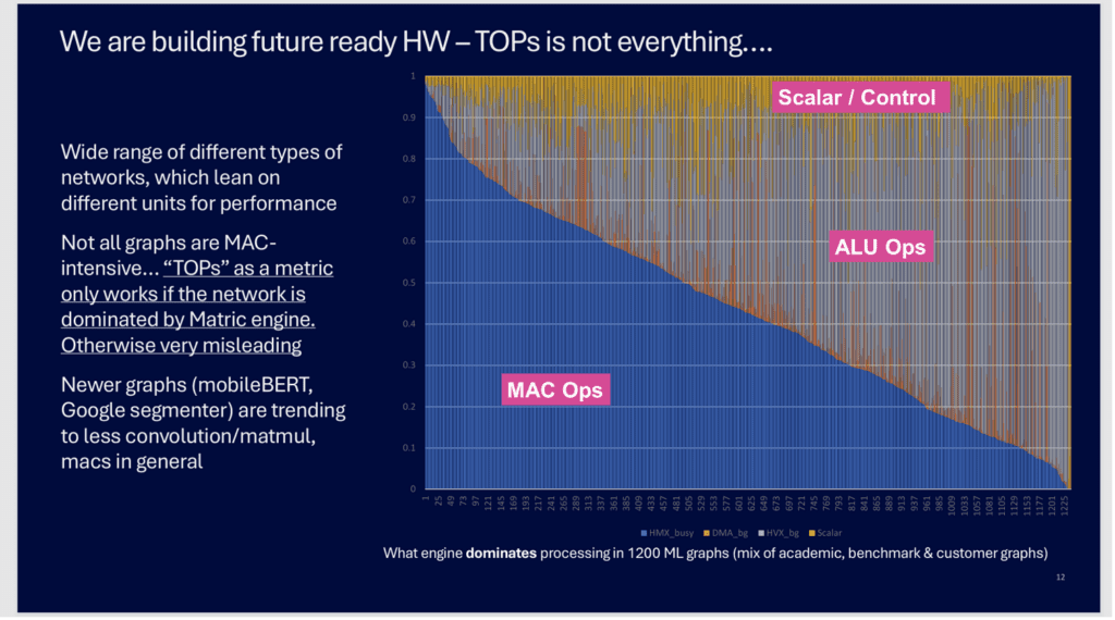
Qualcomm’s Analysis Proves it’s Much More Than MACs
The chart above shows Qualcomm’s analysis of over 1200 different AI/ML networks that they have profiled for their automotive chipsets. The Y axis shows the breakdown of the performance demands for each network, color-coded by how much of the compute is multiply-accumulate (MAC) functions – Blue; other vector DSP type calculations – ALU Operations (Grey, Orange); and pure scalar/control code - Yellow. The 3-segment breakdown by Qualcomm corresponds to how Qualcomm’s Hexagon AI accelerator is designed – with three unique computing blocks.
The first 50+ networks on the lefthand side are indeed MAC dominated, requiring MAC accelerated hardware for >90% of the time. But less than half of the total networks are more than 50% MAC dominated. And some of these newer networks have little or no classical MAC layers at all!
Can You Afford to Use 64 DSPs?
At first blush, the argument made by Qualcomm seems plausible: there is a MAC engine for matrix-dominated networks, and a classic DSP core for networks that are mostly ALU operation bound. Except they leave out two critical pieces of information:
Today’s largest licensable DSPs have 512-bit wide vector datapaths. That translates into 16 parallel ALU operations occurring simultaneously. But common everyday devices – AI PCs and mobile phones – routinely feature 40 TOPs matrix accelerators. That 40 TOP accelerator can produce 2000+ results of 3x3 convolutions each clock cycle. 2000 versus 16. That is a greater than two order of magnitude mismatch. Models run on the DSP are thus two order of magnitude slower than similar models run on the accelerator? Models that need to ping-pong between the different types of compute get bottlenecked on the slow DSP?
Chimera GPNPU – A Better Way!
If silicon area and cost are not a concern, we suppose you could put a constellation of 64 DSPs on chip to make non-MAC networks run as fast as the MAC dominated networks. 64 discrete DSPs with 64 instruction caches, 64 data caches, 64 AXI interfaces, etc. Good luck programming that!
Or, you could use one revolutionary Chimera GPNPU processor that integrates a full-function 32-bit ALU with each cluster of 16 or 32 MACs. Up to 1024 ALUs in a single core, with only one instruction fetch and one AXI data port. Chimera GPNPUs have matched and balanced compute throughput for both MAC and ALU compute so no matter what type of network you choose to run, they all run fast and highly parallel.
No Gimmicks, Just Data
If you want unfiltered, full disclosure of performance data for a leading machine learning processing solution, head over to Quadric’s online DevStudio tool. In DevStudio you will find more than 120 AI benchmark models, each with links to the source model, all the intermediary compilation results and reports ready for your inspection, and data from hundreds of cycle-accurate simulation runs on each benchmark model so you can compare all the possible permutations of on-chip memory size options, assumptions about off-chip DDR bandwidth, and presented with a fully transparent Batch=1 set of test conditions. And you can easily download the full SDK to run your own simulation of a complete signal chain, or a batched simulation to match your system needs.
If you are comparing alternatives for an NPU selection, give special attention to clearly identifying how the NPU/GPNPU will be used in your target system, and make sure the NPU/GPNPU vendor is reporting the benchmarks in a way that matches your system needs.
When evaluating benchmark results for AI/ML processing solutions, it is very helpful to remember Shakespeare’s Hamlet, and the famous line: “To be, or not to be.” Except in this case the “B” stands for Batched.

Batch-1 Mode Reflects Real-World Cases
There are two different ways in which a machine learning inference workload can be used in a system. A particular ML graph can be used one time, preceded by other computation and followed by still other computation in a complete signal chain. Often these complete signal chains will combine multiple, different AI workloads in sequence stitched together by conventional code that prepares or conditions the incoming data stream and decision-making control code in between the ML graphs.
An application might first run an object detector on a high-resolution image to find pertinent objects (people, cars, road obstacles) and then subsequently call on a face identification model (to ID particular people) or a license plate reader to identify a specific car. No single ML model runs continuously because the compute resource is shared across a complex signal chain. An ML workload used in this fashion is referred to as being used in Batch=1, or Batch-1 mode. Batch-1 mode is quite often reflective of real-world use cases.
The Batched Mode Alternative
The alternative is Batched mode, wherein the same network is run repeatedly (endlessly) without interruption. When used in Batched mode, many neural processing units (NPUs) can take advantage of selected optimizations, such as reuse of model weights or pipelining of intermediate results to achieve much higher throughput than the same machine running the same model in Batch-1 mode. Batched Mode can be seen in real world deployments when a device has a known, fixed workload and all the pre- and post-processing can be shifted to a different compute resource, such as a CPU/DSP or a second ML NPU.
Check The Fine Print
Many NPU vendors will only report their Batched results, because there can be substantial Inferences-Per-Second differences between Batch-1 and Batch N calculations. An example screenshot of a popular silicon vendor’s website shows how this Batching “trick” can be presented. Only when the user clicks the Info popup does it become clear that the reported inference time is “estimated” and assumes a Batch mode over an unspecified number of repetitions.

If you have to do a lot of digging and calculations to discover the unbatched performance number, perhaps the NPU IP vendor is trying to distract you from the shortcomings of the particular IP?
How to Get Gimmick-Free Data
If you want unfiltered, full disclosure of performance data for a leading machine learning processing solution, head over to Quadric’s online DevStudio tool. In DevStudio you will find more than 120 AI benchmark models, each with links to the source model, all the intermediary compilation results and reports ready for your inspection, and data from hundreds of cycle-accurate simulation runs on each benchmark model so you can compare all the possible permutations of on-chip memory size options, assumptions about off-chip DDR bandwidth, and presented with a fully transparent Batch=1 set of test conditions. And you can easily download the full SDK to run your own simulation of a complete signal chain, or a batched simulation to match your system needs.
There are a couple of dozen NPU options on the market today. Each with competing and conflicting claims about efficiency, programmability and flexibility. One of the starkest differences among the choices is the seemingly simple question of what is the “best” choice of placement of memory relative to compute in the NPU system hierarchy.
Some NPU architecture styles rely heavily on direct or exclusive access to system DRAM, relying on the relative cost-per-bit advantages of high-volume commodity DRAM relative to other memory choices, but subject to the partitioning problem across multiple die. Other NPU choices rely heavily or exclusively on on-chip SRAM for speed and simplicity, but at high cost of silicon area and lack of flexibility. Still others employ novel new memory types (MRAM) or novel analog circuitry structures, both of which lack proven, widely-used manufacturing track records. In spite of the broad array of NPU choices, they generally align to one of three styles of memory locality. Three styles that bear (pun intended) a striking resemblance to a children’s tale of three bears!
The children’s fairy tale of Goldilocks and the Three Bears describes the adventures of Goldi as she tries to choose among three choices for bedding, chairs, and bowls of porridge. One meal is “too hot”, the other “too cold”, and finally one is “just right”. If Goldi were faced with making architecture choices for AI processing in modern edge/device SoCs, she would also face three choices regarding placement of the compute capability relative to the local memory used for storage of activations and weights.
In, At or Near?
The terms compute-in-memory (CIM) and compute-near-memory (CNM) originated in discussions of architectures in datacenter system design. There is an extensive body of literature discussing the merits of various architectures, including this recent paper from a team at TU Dresen published earlier this year. All of the analysis boils down to trying to minimize the power consumed and the latency incurred while shuffling working data sets between the processing elements and storage elements of a datacenter.
In the specialized world of AI inference-optimized systems-on-chip (SoCs) for edge devices the same principles apply, but with 3 levels of nearness to consider: in-memory, at-memory and near-memory compute. Let’s quickly examine each.
In Memory Compute: A Mirage
In-memory compute refers to the many varied attempts over more than a decade to meld computation into the memory bit cells or memory macros used in SoC design. Almost all of these employ some flavor of analog computation inside the bit cells of DRAM or SRAM (or more exotic memories such as MRAM) under consideration. In theory these approaches speed computation and lower power by performing compute – specifically multiplication – in the analog domain and in widely parallel fashion. While a seemingly compelling idea, all have failed to date.
The reasons for failure are multiple. Start with the fact that widely used on-chip SRAM has been perfected/optimized for nearly 40 years, as has DRAM for off-chip storage. Messing around with highly optimized approaches leads to area and power inefficiencies compared to the unadulterated starting point. Injecting such a new approach into the tried-and-true standard cell design methodologies used by SoC companies has proven to be a non-starter. The other main shortcoming of in-memory compute is that these analog approaches only perform a very limited subset of the compute needed in AI inference – namely the matrix multiplication at the heart of the convolution operation. But no in-memory compute can build in enough flexibility to cover every possible convolution variation (size, stride, dilation) and every possible MatMul configuration. Nor can in-memory analog compute implement the other 2300 Operations found in the universe of Pytorch models. Thus in-memory compute solutions also need to have full-fledged NPU computation capability in addition to the baggage of the analog enhancements to the memory – “enhancements” that are an area and power burden when using that memory in a conventional way for all the computation occurring on the companion digital NPU.
In the end analysis, in-memory solutions for edge device SoC are “too limited” to be useful for the intrepid chip designer Goldi.
Near Memory Compute: Near is still really very far away
At the other end of the spectrum of design approaches for SoC inference is the concept of minimizing on-chip SRAM memory use and maximizing the utilization of mass-produced, low-cost bulk memories, principally DDR chips. This concept focuses on the cost advantages of the massive scale of DRAM production and assumes that with minimal on-SoC SRAM and sufficient bandwidth to low-cost DRAM the AI inference subsystem can lower SoC cost but maintain high performance by leaning on the fast connection to external memory, often a dedicated DDR interface solely for the AI engine to manage.
While successful at first glance at reducing the SoC chip area devoted to AI and thus slightly reducing system cost, near-memory approaches have two main flaws that cripple system performance. First, the power dissipation of such systems is out of whack. Consider the table below showing the relative energy cost of moving a 32bit word of data to or from the multiply accumulation logic at the heart of every AI NPU:
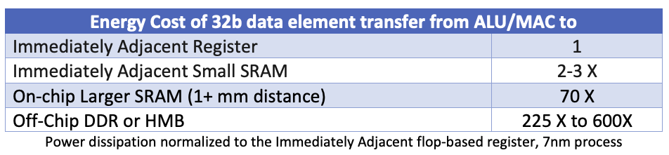
Each transfer of data to or from the SoC to DDR consumes between 225 to 600 times the energy (power) of a transfer that stays locally adjacent to the MAC unit. Even an on-chip SRAM a considerable “distance” away from a MAC unit is still 3 to 8 times more energy efficient than going off-chip. With most such SoCs power-dissipation constrained in consumer-level devices, the power limitations of relying principally on external memory renders the near-memory design point impractical. Furthermore, the latency of always relying on external memory means that as newer, more complicated models evolve that might have more irregular data access patterns than old-school Resnet stalwarts, near-memory solutions will suffer significant performance degradation due to latencies.
The double whammy of too much power and low performance means that the near-memory approach is “too hot” for our chip architect Goldi.
At-Memory: Is Just Right
Just as the children’s Goldilocks fable always presented a “just right” alternative, the At-Memory compute architecture is the solution that is Just Right for edge & device SoCs. Referring again to the table above of data transfer energy costs the obvious best choice for memory location is the Immediately Adjacent on-chip SRAM. A computed intermediate activation value saved into a local SRAM burns up to 200X less power than pushing that value off-chip. But that doesn’t mean that you want to only have on-chip SRAM. To do so creates hard upper limits on model sizes (weight sizes) that can fit in each implementation.
The best alternative for SoC designers is a solution that both take advantage of small local SRAMs – preferably distributed in large number among an array of compute elements – as well as intelligently schedules data movement between those SRAMs and the off-chip storage of DDR memory in a way that minimizes system power consumption and minimizes data access latency.
The Just Right Solution
Luckily for Goldilocks and all other SoC architects in the world, the is such a solution: Quadric’s fully programmable Chimera GPNPU – general purpose NPU – a C++ programmable processor combining the power-performance characteristics of a systolic array “accelerator” with the flexibility of a C++ programmable DSP. The Chimera architecture employs a blend of small distributed local SRAMs along with intelligent, compiler-scheduled use of layered SRAM and DRAM to deliver a configurable hardware-software solution “just right” for your next Soc. Learn more at: www.quadric.io.
The biggest mistake a chip design team can make in evaluating AI acceleration options for a new SoC is to rely entirely upon spreadsheets of performance numbers from the NPU vendor without going through the exercise of porting one or more new machine learning networks themselves using the vendor toolsets.
Why is this a huge red flag? Most NPU vendors tell prospective customers that (1) the vendor has already optimized most of the common reference benchmarks, and (2) the vendor stands ready and willing to port and optimize new networks in the future. It is an alluring idea – but it’s a trap that won’t spring until years later. Unless you know today that the Average User can port his/her own network, you might be trapped in years to come!
Rely on NPU Vendor at Your Customers’ Customers Expense!
To the chip integrator team that doesn’t have a data science cohort on staff, the daunting thought of porting and tuning a complex AI graph for a novel NPU accelerator is off-putting. The idea of doing it for two or three leading vendors during an evaluation is simply a non-starter! Implicit in that idea is the assumption that the toolsets from NPU vendors are arcane, and that the multicore architectures they are selling are difficult to program. It happens to be true for most “accelerators” where the full algorithm must be ripped apart and mapped to a cluster of scalar compute, vector compute and matrix compute engines. Truly it is better to leave that type of brain surgery to the trained doctors!
But what happens after you’ve selected an AI acceleration solution? After your team builds a complex SoC containing that IP core? After that SoC wins design sockets in the systems of OEMs? What happens when those systems are put to the test by buyers or users of the boxes containing your leading-edge SoC?
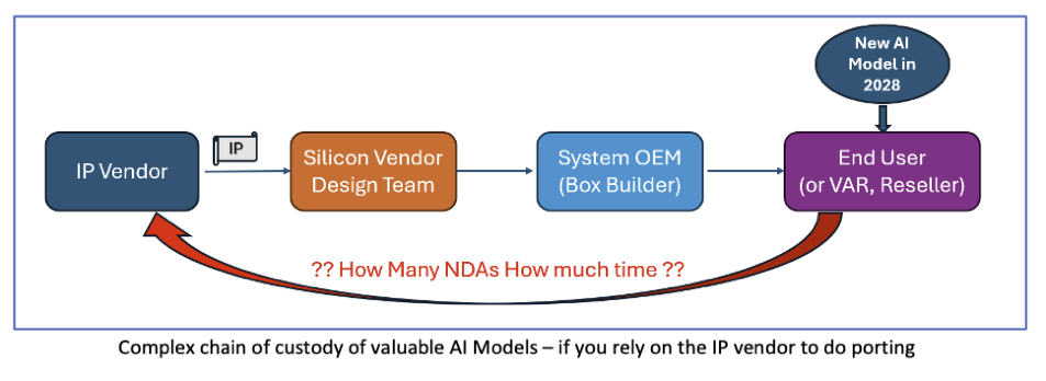
Who Ports and Optimizes the New AI Network in 2028?
The AI acceleration IP selection decision made today – in 2024 – will result in end users in 2028 or 2030 needing to port the latest and greatest breakthrough machine learning models to that vintage 2024 IP block. Relying solely on the IP vendor to do that porting adds unacceptable business risks!
Layers Of Risk
Business Relationship Risk: Will the End User – likely with a proprietary trained model – feel comfortable relying on a chip vendor or an IP vendor they’ve never met to port and optimize their critical AI model? What about the training dataset? If model porting requires substituting operators to fit the limited set of hardwired operators in the NPU accelerator, the network will need to be retrained and requantized – which means getting the training set into the hands of the IP vendor?
Legal Process Risk: How many NDAs will be needed – with layer upon layer of lawyer time and data security procedures – to get the new model into the hands of the IP vendor for creation of new operators or tuning of performance?
Porting Capacity Risk: Will the IP vendor have the capacity to port and optimize all the models needed? Or will the size of the service team inside the IP vendor become the limiting factor in the growth of the business of the system OEM, and hence the sales of the chips bearing the IP?
Financial Risk: IP vendor porting capacity can never be infinite no matter how eager they are to take on that kind of work – how will they prioritize porting requests? Will the IP vendor auction off porting priority to the “highest bidder”? In a game of ranking customers by importance or willingness to write service fee checks, someone gets shoved the end of the list and goes home crying.
Survivor Risk: The NPU IP segment is undergoing a shakeout. The herd of more than twenty would-be IP vendors will be thinned out considerably in four years. Can you count on the IP vendor of 2024 to still have a team of dedicated porting engineers in 2030?
In What Other Processor Category Does the IP Vendor Write All the End User Code?
Here’s another way to look at the situation: can you name any other category of processor – CPU, DSP, GPU – where the chip design team expects the IP vendor to “write all the software” on behalf of the eventual end user? Of course not! A CPU vendor delivers world-class compilers along with the CPU core, and years later the mobile phone OS or the viral mobile App software products are written by the downstream users and integrators. Neither the core developer nor the chip developer get involved in writing a new mobile phone app! The same needs to be true for AI processors – toolchains are needed that empower the average user – not just the super-user core developer - to easily write or port new models to the AI platform.
A Better Way – Leading Tools that Empower End Users to Port & Optimize
Quadric’s fully programmable GPNPU – general purpose NPU – is a C++ programmable processor combining the power-performance characteristics of a systolic array “accelerator” with the flexibility of a C++ programmable DSP. The toolchain for Quadric’s Chimera GPNPU combines a Graph Compiler with an LLVM C++ compiler – a toolchain that Quadric delivers to the chip design team and that can be passed all the way down the supply chain to the end user. End users six years from now will be able to compile brand new AI algorithms from the native Pytorch graph into C++ and then into a binary running on the Chimera processor. End users do not need to rely on Quadric to be their data science team or their model porting team. But they do rely on the world-class compiler toolchain from Quadric to empower them to rapidly port their own applications to the Chimera GPNPU core.