Quadric's GPNPU delivers benefits to both SoC developers and downstream software programmers, speeding both chip design and application development.
Artificial Intelligence (AI) enhances the functionality of devices used in many applications – autonomous vehicles, industrial robots, remote controls, game consoles, smartphones, and smart speakers just to name a few applications that put AI to good use. Machine Learning (ML) is a subset of the broader category of AI. By using ML models, which are trained by sifting through enormous amounts of historical data to discover patterns, devices can perform amazing tasks without being explicitly programmed.
ML models are created using known labeled datasets (training phase) and are subsequently used to make predictions when presented with new, unknown data in a live deployment scenario (inference). Because an enormous amount of computing resources is required both for training and inference, specialized processors have been designed to handle ML computational workloads in both datacenters and devices. In general, these processors can be divided into “accelerators” that are coupled with a fully programmable processor to offload parts of the ML workload and “neural processing units” (NPUs) that are fully programmable to handle a complete ML workload.
While dedicated ML chips often make economic sense in the hyperscaler datacenter use case, for most high-volume consumer products cost, power, and size limitations rule out discrete ML processor chips. Instead, chips with built-in ML processing horsepower in the form of licensed semiconductor IP building blocks are the best option.
What are the choices and trade-offs when considering available ML processor options for new system on chip (SoC) designs?
Figure 1 represents a conceptual block diagram of an ML-enabled high-performance camera-enabled SoC utilizing the conventional approach to deploying embedded computing resources. As workloads have evolved over the past two decades and as Moore’s law has enabled ever higher levels of integration, conventional architectures have accumulated a wide array of specialized processing building blocks.
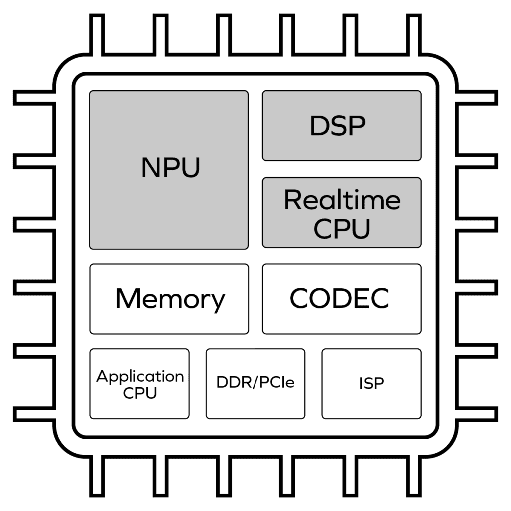
It’s important to briefly touch on the responsibilities of several of these key building blocks that impact the ML performance of an SoC:
An NPU accelerates compute-intensive, matrix-math ML workloads. NPUs are optimized to handle matrix multiplication blazingly fast but usually cannot run any code other than the ML graph code they were specifically optimized to run. Most NPUs today are essentially large arrays of hardwired, fixed-point multiply-accumulate (MAC) blocks running in parallel. Most NPUs in silicon today can only support a few dozen common neural network operators (or “graph layers”) – a handful each of convolution, pooling, and activation layers – among hundreds of operator types backed by the leading training frameworks such as Tensorflow and PyTorch.
The graph layers running on the NPU usually comprise 90-95%of the expected compute cycles consumed in today’s most popular ML networks, and thus these ML accelerators do an admirable job of handling today’s known inference workloads. Other less performance-critical operators are partitioned to run on the other processor engines in the system, delivering acceptable system performance at the cost of upfront engineering effort. These accelerator NPUs cannot run all layer types – and are not fully programmable processors- therefore they likely cannot run new layers that have not yet been invented by the data scientists who continue to rapidly evolve the state-of-the-art of machine learning. For layers that don’t run on the NPU, the existing approach to delegate these layers to other cores in the system is typically a manual and time-consuming partitioning problem that demands the software programmer have an intimate understanding of the target chip. If a developer needs to target different devices each with a different NPU accelerator, that partitioning exercise needs to be repeated for each new silicon target – a time consuming approach.
DSPs are vector processor cores intended to handle a wide variety of complex math operations efficiently. They are widely used in various applications requiring signal processing – voice or image pre-processing are prime examples.
DSPs can be used to handle some matrix computations, but they are not optimized for them and tend to be inefficient compared to the matrix-optimized NPU accelerators described previously. Additionally, DSPs are typically highly utilized in the system running more conventional C code for signal pre- and post-processing, and thus have little performance headroom to handle heavy matrix computation. Therefore DSPs in most SoCs can augment the NPUs and run some but not all ML graph operators that the NPU doesn’t nativelyh handle.
The realtime CPU is responsible for controlling the overall inference functionality in the SoC. It coordinates ML inference workloads between the NPU, DSP, and the memory (used to store model weights). The realtime CPU is often the only programmable core in the inference subsystem that is exposed to the programmer. Because building and deploying multicore software development kits (SDKs) is a complex task, and because using a multicore SDK requires a complex learning cycle, most semiconductor vendors who employ CPU+DSP+NPU inference subsystems only expose the CPU to the developer for developer code, providing access to the DSP and NPU only via prebuilt application programming interfaces (APIs). If a developer needs an ML operator not supported in the APIs for the NPU or DSP, they can add a new ML operator on the CPU but generally not on the NPU or DSP.
Because CPUs are general purpose, they can functionally run any code the programmer desires, but because they lack the vector performance of a DSP or the matrix performance of an NPU, CPUs are poor performers for new ML operators. The programmer thus must choose between high-performance ML operators prebuilt with published APIs or slow ML operators added to the CPU.
Distinctions must be made between the realtime CPU and an application-class CPU, both of which are shown in the conceptual block diagram above. The latter is the larger CPU core running a complex operating system such as Linux, the application, and many other managerial functions. It usually has little involvement in real-time-sensitive ML computations.
The following are just a few challenges that SoC developers are faced with and how they are presently addressed:
Building SoCs that can handle known challenges is a good start but insufficient. The real challenge is to develop devices that are flexible enough to support some range of future requirements.
ML technology is evolving rapidly. New models, libraries, and operators are introduced at a rapid pace. This makes it essential to develop devices optimized for ML inference that can be programmed to support new operators and algorithms when they become available.
The existing heterogeneous SoC architecture approach described above is often not flexible enough to support new operators with the performance required. This is due to the inflexibility of hardwired NPUs that cannot be reconfigured. Developers tackle this challenge by adding code to the DSP or the realtime CPU to compensate for the NPU’s shortcomings.
This approach is suboptimal in performance and creates a new set of problems. For example, splitting matrix operations between two disparate cores (NPU and CPU) penalizes inference latency and power dissipation since large data blocks have to traverse the chip going from one core to the other.
Dealing with multiple IP cores from multiple IP vendors invariably leads to reliance on multiple toolsets, creating many challenges. It is exceedingly difficult to debug a system using more than one debugger. As an example, it is challenging to find quick answers to common debugging questions such as:
· Where is the system bottleneck?
· Why can’t I get the throughput that I expected?
· Why does inference latency vary so drastically
· Is this problem a software bug or hardware issue?
Presently there are no easy ways to address this problem. Diversity in toolsets invariably leads to longer development times.
Designers need a new AI acceleration processor architecture designed from the ground up to address the significant ML inference deployment challenges facing SoC developers. Quadric’s General Purpose Neural Processing Unit (GPNPU) is a simple yet powerful architecture with demonstrated improved matrix-computation performance than the traditional approach. Its crucial differentiation is its ability to execute diverse workloads with great flexibility all on a single machine.
The Quadric GPNPU is a unified processor architecture that handles matrix operations, vector operations and scalar (control) code in one execution pipeline. These workloads are traditionally handled separately by the NPU, DSP, and real-time CPU. The entire GPNPU architecture is abstracted to the user as a single software-controlled core, allowing for the simple expression of complex parallel workloads.
The Quadric GPNPU is entirely driven by code, empowering developers to continuously optimize the performance of their models and algorithms throughout the device’s lifecycle.
Figure 2 is the conceptual block diagram of the same camera-enabled SoC based on Quadric’s architecture. The significance of this arrangement is that the GPNPU can singlehandedly run workloads traditionally run independently on the DSP, NPU, and real-time CPU cores.
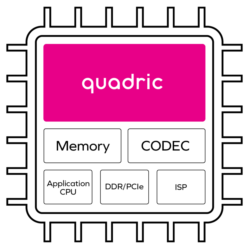
Figure 3 is a comparison of the traditional approach with this new approach based on a GPNPU.
Figure 3. A comparison of the traditional approach (left) and the Quadric GPNPU approach
The benefits of using a GPNPU are:
Quadric’s solution enables hardware developers to instantiate a single core that can handle an entire ML workload plus the typical DSP pre-processing and post-processing, signal conditioning workloads often intermixed with ML inference functions. Dealing with a single core drastically simplifies hardware integration and eases performance optimization. System design tasks such as profiling memory usage to ensure sufficient off-chip bandwidth are greatly simplified.
Quadric’s GPNPU architecture dramatically simplifies software development since matrix, vector, and control code can all be handled in a single code stream. ML graph code from the common training toolsets(Tensorflow, Pytorch, ONNX formats) is compiled by the Quadric toolset and merged with signal processing code written in C++, all compiled into a single code stream running on a single processor core.
Quadric’s toolset meets the demands of both hardware and software developers, who no longer need to master multiple toolsets from multiple vendors. The entire subsystem can be debugged in a single debug console. This dramatically reduces code development time and eases performance optimization.
This new programming paradigm also benefits the end users of the SoCs since they will have access to program all the GPNPU resources.
A Quadric GPNPU can run anything written in C++. This is incredibly powerful since SoC developers can write code to implement new neural network operators and libraries long after the SoC has been taped out. This eliminates fear of the unknown future ML operator and dramatically increases a chip’s useful life.
Again, this flexibility is extended to the end users of the SoCs. They can continuously add new features to the end products, giving them a competitive edge.
Replacing the heterogenous ML subsystem comprised of separate NPU, DSP, and real-time CPU cores with one GPNPU has potent advantages. By allowing vector, matrix, and control code to be handled in a single code stream, the development and debug process is greatly simplified while the ability to add new algorithms efficiently is greatly enhanced.
As ML models continue to evolve and inferencing becomes prevalent in even more applications, the payoff from this unified architecture helps future proof chip design cycles.
In this blog post, quadric explores the acceleration of the Non-Maximal Suppression (NMS) algorithm used by object detection neural networks such as Tiny Yolo V3. We dive into the challenges of accelerating NMS, and why quadric's approach results in best-in-class performance.
When pushed to the limit of a network, the need for accelerated processing in resource-constrained settings becomes a complex problem to solve. That is where the quadric architecture comes into play. Our architecture's combination of 4 TeraOPS (TOPS) per second and 4 million-Million Instructions Per Second (MIPS) is well-suited for accelerating an entire application pipeline at the edge. MIPS is a standard measure of a CPU's speed, while TOPS is a common measure of the capability of a Neural Network accelerator. Striking a balance between these two is critical for total algorithm performance. To demonstrate this, let's take a look at a basic example: YOLO.
You might think that since YOLO is a neural network, it can be accelerated with an NPU and the TOPS it provides in its entirety. However, this isn't the case. And the reason is not apparent. To enable a neural-network-based object detection algorithm to have clean detection, we need the help of a classical algorithm: Non-Maximal Suppression, or NMS for short.
Non-maximal suppression is a critical step in detecting objects in an image. NMS is a classical algorithm that analyzes detection candidates and keeps only the best ones. However, it is computationally expensive, making it difficult to accelerate with traditional hardware architectures. The quadric architecture addresses problems like this, and it delivers the performance necessary for resource-constrained edge performance. Our approach makes it well-suited for accelerating the entire application pipeline, including but not limited to non-maximal suppression.
YOLO is a detection algorithm that can know if things are in an image and where. It does this by looking at the picture and deciding what it might see, for example, a person, a car, or a cat. To illustrate how detection algorithms work, let’s enlist the help of my puppy, Maverick.
A classifier algorithm may identify a dog in the photo, but it does not always indicate where in the image the pup is.
On the other hand, a localization algorithm would only tell you that something is in a position in the photograph.
A detection algorithm will tell you a dog is in a specific image region. YOLO is one such detection algorithm.
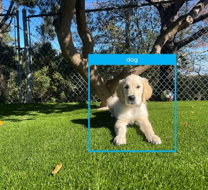
YOLO produces a set of candidate bounding boxes around objects in an image – the boxes in which it has sufficiently high confidence that they represent the most probable dimensions and location of a recognized entity.
YOLO is more discerning than other image classification methods. It produces far fewer bounding boxes for a given object detected, and it’s faster. Let's look at YOLO in more detail. To perform the complete algorithm, technically, there are two steps:
Let's start at the end: here is a nice clean image of a final detection that one would expect to see after YOLO completes a detection on an image. Dog, ball, tree. Super easy! Let’s see what it takes.
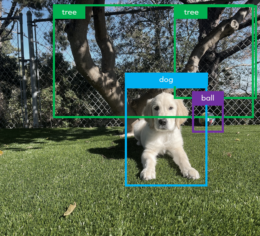
The TOPs-accelerate able NN backbone produces a set of best-guesses in the form of multiple bounding boxes, each offset around a given object, each with varying dimensions inferred by the math. Here again is Maverick framed by several bounding boxes that represent YOLOs best guesses about the sizes and probable positions of the dog in the image:

But this is as far as a TOPs-only approach using neural networks can take us.
To pick the “best” box and complete the detection pipeline, we need suppression to sort boxes by their score and toss out overlapping and otherwise low-scoring boxes. The most widely used algorithm is NMS. YOLO includes NMS as a final step, as do most other detection algorithms.
So we know we need NMS. But how does it work?
NMS is a less celebrated component of the recognition pipeline. Maybe because it’s a simple, classic algorithm – or because it’s not even AI. Or perhaps it is because it is the elephant in the room: NMS is a classical algorithm that is hard to accelerate.
But that’s what makes its implementation so challenging. It’s “normal” code, built with compares, branches, loops with dynamic termination conditions, 2d geometry, and scalar math. It doesn’t run natively on an NPU and is difficult to accelerate on a GPU. NMS acceleration on a TOPs-accelerating NPU is impossible, and NMS’s acceleration on the GPU is an active research topic. NMS goes something like this:
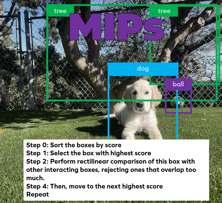
NMS may be straightforward code-wise, but it’s a critical path component that runs in every major iteration of the detection pipeline.
Consider the NMS implementations in TensorFlow. It provides both CPU and GPU versions, which is nice, but the GPU and CPU implementations run at about the same speed under normal conditions. State-of-the-art NMS computation execution latencies are on the order of 5-10 ms. These execution latencies are on the order of what most people would consider the more computationally intensive portion: the neural backbone. Most implementations: execute the neural backbone on an NPU or GPU, transfer the data over to a powerful CPU host, and implement NMS there. With the quadric architecture, you would already be done.
Looking at tiny YOLO v3 on our q16, the entire algorithm breaks down like this:
Consuming only 2W on the quadric Dev Kit and clocking in at 7ms, NMS contributes only 4% of the total execution time. In similar deployments, NMS can consume up to 50% of the total execution time. The best NMS implementation that we could find is a 2ms desktop-class GPU implementation. Most edge implementations range from 10ms to 100ms depending on input image size and characteristics of the hardware.
The critical point is that these algorithms, the neural backbone, and the classical NMS are chained back to back. The Neural Network Backbone completes, and the NMS starts immediately in place. There is no need for data transfers to specialized hardware or back to a powerful host. Whether deployed alongside a powerful x86 or a simple raspberry pi, the performance remains constant.
This concept, when generalized, can lead to some inspiring possibilities. Chain further beyond NMS to predict what will happen next. Entire application pipelines are possible on our processor architecture. We built our technology not to accelerate a single slice of an application pipeline but to accelerate as much of it as possible. We believe that this has enormous potential in resource-constrained deployments.
Computer vision, and particularly our object recognition example, demonstrates the power of the TOPs + MIPs approach. But it’s just one of many use cases that illustrate the value of quadric’s more holistic approach to edge computing.
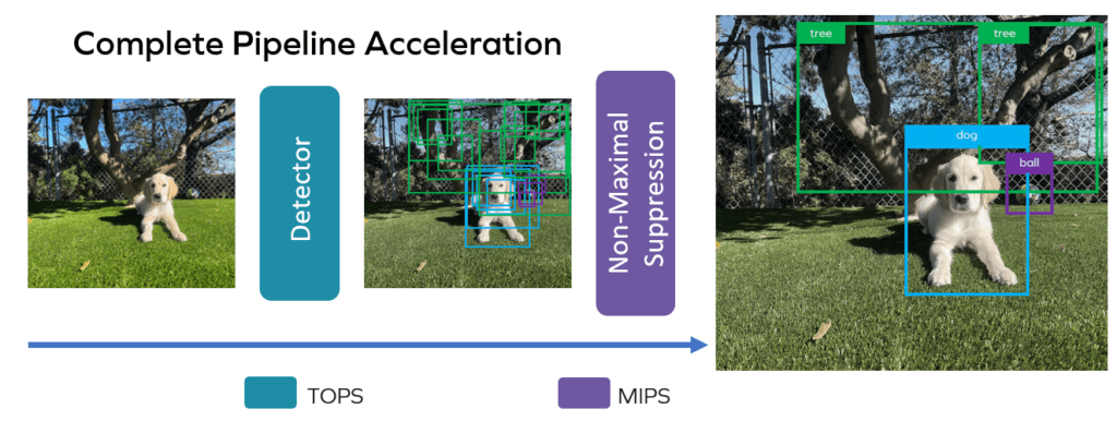
In upcoming editions of our blog series, we’ll explore more capabilities of the quadric platform and look at how extensively its support for MIPs functionality is. That means support for algorithms that remain critical across many applications at the edge.
A few links:
https://hertasecurity.com/wp-content/uploads/work-efficient-parallel-non-maximum-suppression.pdf
https://arxiv.org/ftp/arxiv/papers/2108/2108.07939.pdf
https://github.com/gdlg/pytorch_nms
https://whatdhack.medium.com/reflections-on-non-maximum-suppression-nms-d2fce148ef0a
We want to drive home the point that along with Neural Network acceleration, we also accelerate data parallelism for classical algorithms, as well. We selected the Fourier Transform because of its historical and continued importance across many industries. As well as the elegance with which is maps to our architecture.
Next up in our algorithm stories series, we want to walk you through how more general-purpose, highly parallelizable algorithms map to our architecture. In this installment, we will talk about one of the most important algorithms of all time, the Fourier transform. An algorithm with its origins in the early 19th century to describe heat propagation in solid bodies, its applications are wide-ranging.
Let’s focus on the implementation and acceleration of the FFT using our Source Mode. If you want to learn more about the FFT itself and its applications, I’ve included a list of my favorite resources below. My personal favorite is the “Three Blue One Brown” video on the Fourier transform.
https://en.wikipedia.org/wiki/Fourier_transform
https://en.wikipedia.org/wiki/Fourier_analysis
If you take away only one thing about the universal application of the FFT, look no further than in your pocket. Modern radio communications rely heavily on frequency domain representation of real-world sampled data. And the way that we get a frequency domain representation of that data is by using the FFT.
With that motivation, let’s get started with a simple example. Consider the time-domain representation of my voice:
This is a voice recording of me saying, “ the FFT is cool.” You can see it takes me about 1.5 seconds to say that. But what is the average frequency composition of voice for these 1.5 seconds? Using the FFT, we can generate a frequency domain representation. Here we plot the amplitude of a signal versus its frequency composition.
According to Wikipedia: the human male voice can produce frequencies from 85 to 180 Hz. So it looks like it checks out!
To generate the FFT, we will look at the Cooley Tukey algorithm developed in the mid 20th century. This algorithm completes the FFT in O(n*log(n)) and is well suited to map the quadric processor architecture.
For illustration purposes, we can take a sample or “window” from my audio recording consisting of 8 points. By taking an 8 sample window, we will effectively be performing an “8-Point FFT.” For ease of explanation and the sake of illustration, we will map the FFT on a 2x2 architecture instance. That’s a vector that has shape 8x1:
A = [-0.00064087 -0.00062561 -0.00074768 -0.00068665 -0.00065613 -0.00054932 -0.0005188 -0.00061035]
To implement the FFT algorithm, we will following these steps:
We can remap the data inside of our array using index manipulation. Reversing the index arrives at the desired remapping. Have a look at the effect on an 8 point FFT. The same will be valid for any arbitrary power of 2 - point implementation.
The code for such remapping looks something like this:
template
INLINE void fetchInputIndexBitReversed(OcmInOutSignalTensorShape ocmIn,
qVar_t qInput[],
std::int32_t signalRowOffset = 0,
std::int32_t signalChOffset = 0) {
constexpr std::int32_t numTilesPerInputPoints =
roundUpToNearestMultiple(inputPoints, Epu::numArrayCores) / Epu::numArrayCores;
Rau::config(ocmIn);
qVar_t qLocalCoreIndx = qRow<> * Epu::coreDim + qCol<>;
constexpr std::int32_t complexCount = 2; // real and imaginary
for(std::uint32_t chIndx = 0; chIndx < complexCount; chIndx++) {
for(std::uint32_t tileIndx = 0; tileIndx < numTilesPerInputPoints; tileIndx++) {
qVar_t coreIndx = tileIndx * Epu::numArrayCores + qLocalCoreIndx;
qVar_t rCoreIndx = bitReversal(coreIndx);
std::int32_t arrayIndx = chIndx * numTilesPerInputPoints + tileIndx;
qInput[arrayIndx] = Rau::Load::oneTile(0, signalChOffset + chIndx, signalRowOffset, rCoreIndx, ocmIn);
if(coreIndx >= inputPoints) {
qInput[arrayIndx] = 0;
}
}
}
}
The above data remapping leads to a rearrangement of the vector in the following fashion:
The rearranged input vector is on the left. And the output vector is shown on the right after the Cooley-Tukey algorithm is applied.
If you were to implement the algorithm as matrix multiplication, with 3 matrix products of sparse representations. You would think this would lead to poor spatial array utilization. However, we can pack the products and share data cleverly to execute the algorithm efficiently.
Let’s simplify our representation of the quadric architecture into 4 simple rectangles. Each representing a Vortex Core. Any variable depicted within the rectangle is stored locally within that Vortex Core’s local memory.
Using the periphery load-store units. We write the remapped vector linearly L-R, T-B into the core. When we’ve reached the end, we return to the upper left Vortex Core and then write the L-R, T-B. In our simple case of an 8-point FFT mapping to a 4 core architecture instance, this results in the following data layout:
Now we can execute the stage 1 product using neighboring data. If we look at the top row, we need to complete the product a0 + W0*a4 and a1 + W0*a5. The inputs a0 and a1 are stored locally. While the inputs a4 and a5 are stored in our nearest neighbors. The opposite is true for the core the east of it (upper right core). Using single cycle neighbor access, we can publish our data to our neighboring Vortex Cores and consume them in our own product. You can think of the first stage mapping of the 8-point 1D FFT as mapping to row-wise data sharing.
Now we can execute the stage 2 products using neighboring data. If we look at the top row again, we need to perform the products of the subsequent stage with information now stored in our North-South neighbors. So we can publish the intermediate values north and south to be used in that computation. You can think of the second stage mapping of the 8-point 1D FFT as mapping to column-wise data sharing.
For the third and final stage, notice that the required data has been folded inside each Vortex Core. The information is stored locally inside of the register file of the Vortex Core that needs it. So to complete the final products, we can simply fetch the intermediate products stored locally to finish out the FFT. You can think of the third stage mapping of the 8-point 1D FFT as mapping to depth-wise or channel-wise data sharing.
The 8-point FFT is now completed. The upper left core stores the A0 and A1, the upper right Vortex Core containing A4 and A5, the lower-left Vortex Core containing A2 and A3, and the final core containing A6 and A7. We chose this combination of array size and FFT-point window because it covers all cases that arise in other varieties. No matter what, there will be some combination of row-wise, column-wise, and channel-wise data sharing.
Here is a short animation of the above description!
We have generalized the concept for all N-point variants based upon the dimensionality of the core array. Of course, running an N-point FFT on the q16 processor would be easy. However, the q16 will process a 512 point FFT similarly to the example we walked through today. Instead of 3 stages, it would require 9. As a part of the quadric SDK, we provide FFT library calls that handle the data manipulation. Here is a snippet of the relevant source for determining the layout. We present this as an example to give you an idea of the power and compatibility of our high-performance data-parallel processing architecture. For more information about the 1D FFT library function, check out our documentation :
1DFFT library definition on docs.quadric.io
The first in a series of Algorithm Stories.
In this blog post, the first in a series, we would like to reinforce the idea that our architecture is code-driven. On our architecture overview page, we have a designed an animated sequence that abstracts and introduces the main features of our instruction set architecture. Let’s have a look at some of those features in more detail. Here we look at the animated sequence and address each part and see how we will control it with basic SDK API calls. Expect more from the series in the future. But first, we will start with a simple example to show the power of the Source Mode features of the quadric SDK.
Large local memories offer the developer space for large data structures. Multiple ports allow for simultaneous reading and writing to keep the vortex core array busy.
The cores in the same architecture group get the same instruction. Let’s look at the following block of code:
#define NUM_TIMES = 10;
qVar_t <std::int32_t> qData[NUM_TIMES];
for(std::int32_t count = 0; count < NUM_TIMES; count++) {
qData[count] += 2 * count;
}
In this block of code, qvar qData is being declared in each core at the same time. We define NUM_TIMES as 10, and the corresponding data structure inside of each Vortex Core is 10 entries deep. The compiler will allocate space for it in the local RF, and each Core’s address will be the same. For a 256 Vortex Core architecture like the one on the q16 Processor, this is 2560 total unique variables, 10 for each core. We compute the value of each entry of qData to 2 times the loop variable. 2 * count is happening 256 times, at the same time, for each loop iteration.
What if we want subgroups of cores to do slightly different things? We achieve this through an architectural feature called prediction. Predication allows us to use the dynamic runtime information from any variable present in the architecture to change the behavior of our program execution. This can also be used to implement compute-sparsity or early loop termination.
Continuing to build, we want even columns to do something slightly differently from odd columns. Instead of multiplying the iteration count by a constant, we now take information from our nearest neighboring Vortex Core. In the case of even columns, the result will be passed to the east. While in the case of the odd columns, the product will be given to the west.
We can do something simple: update the value of a variable by multiplying the value of a loop variable with a value from the physically neighboring Vortex Core. We receive this value from the East for even columns, and we pass our value to the West. For odd columns, we do the opposite. Each Vortex Core has knowledge of its physical placement. We conditionally branch based on whether the column is even or odd. Here is the resulting code:
#define NUM_TIMES = 10;
qVar_t<std::int32_t> qData[NUM_TIMES];
for(std::int32_t count = 0; count < NUM_TIMES; count++) {
qWest<> = qData[count];
qEast<> = qData[count];
if(qCol<> % 2 == 0) {
// the column of the core is even
qData[count] += qEast<> * count;
} else {
// the column of the core is odd
qData[count] += qWest<> * count;
}
}
With this simple example, we see the power of predication against a single instruction for every Vortex Core in an architecture group. In addition to that, we see how multi-directional data flow can be programmed within the Array itself. To tie it back to the architecture visualization, here is what is happening in terms of data flow:
Edge load-store units are static and completely software-controlled, allowing for deterministic kernel runtimes. Each edge has a load-store unit, unlocking novel software API possibilities such as native data rotations and data remapping.
Let’s address how the data arrived at the cores in the first place. And, more importantly, how the developer controls those functions. Data flow is an important concept when discussing any dense data algorithm running on a parallel architecture. Ensuring data reuse and minimizing data movements will lead to optimal overall algorithm performance and minimized power consumption.
Our load-store units can load into the Array or store from the Array from any side. We can load from one side at the same time we store in the other. This allows for a good deal of generalized algorithmic possibilities but let’s look at a simple case: loading data into the array from the North while storing data into OCM via the South.
qVar_t<std::int32_t> qData[OcmInOutShape::NUM_TILES];
fetchAllTiles<IteratorType::YX_NO_BORDER>(ocmInp, qData);
// Add Neighbors
for(std::int32_t tileNum = 0; tileNum < OcmInOutShape::NUM_TILES; tileNum++) {
qWest<> = qData[tileNum];
qEast<> = qData[tileNum];
qBroadcast<0, std::int32_t, BroadcastAction::POP>
if(qCol<> % 2 == 0) {
// the column of the core is even
qData[tileNum] += qEast<> * tileNum + qBroadcast<0, std::int32_t>
} else {
// the column of the core is odd
qData[tileNum] += qWest<> * tileNum + qBroadcast<1, std::int32_t>
}
}
// Flow out data
writeAllTiles<IteratorType::YX_NO_BORDER>(qData, ocmOut);
fetchAllTiles is an iterator in the SDK. The basic idea is these iterators will iterate through multi-dimensional tensors with a particular convention, in this case, YX, and send that data into 2-dimensional slices that can be mapped into the Array itself. Once we have complete the compute, we have a call to writeAllTiles that does the reverse, storing the qData Array variables to the on-chip memory. An important thing to note is that the main loop, in this case, is now done OcmInOutShape::NUMTILES times, which corresponds to the number of 2D YX slices that exist in the tensor ocmInp. Our compiler takes any opportunity to overlap the previous writeAllTiles command with the subsequent fetchAllTiles command in the outer kernel loop.
This results in a visualization that looks something like this:
We have an section in the docs on iterators and Load/Store control. https://docs.quadric.io/templates/api/ocm-array.html
Large local memories offer the developer space for large data structures. Multiple ports allow for simultaneous reading and writing to keep the vortex core array busy.
Another essential thing to note is the architecture comes with a configurable size on-chip memory. The memory is configured to enable at least 1 simultaneous read and write. On the q16 Processor, the architecture instance contains an 8MB memory configured into 4 slices with 1 simultaneous read and 1 simultaneous write possible. The memory is large enough to hold data structures such as frame buffers, neural network weights, more significant intermediary dynamic memory, etc.
typedef DdrTensor<std::int32_t, 1, 1, (1 * Epu::coreDim), (3 * Epu::coreDim)> DdrInOutShape;
typedef OcmTensor<std::int32_t, 1, 1, (1 * Epu::coreDim), (3 * Epu::coreDim)> OcmInOutShape;
EPU_ENTRY void even_odd_example_int32(DdrInOutShape::ptrType ddrInpPtr,
DdrInOutShape::ptrType ddrOutPtr) {
MemAllocator ocmMem;
DdrInOutShape ddrInp(ddrInpPtr);
DdrInOutShape ddrOut(ddrOutPtr);
OcmInOutShape ocmInp;
ocmMem.allocate(ocmInp);
OcmInOutShape ocmOut;
ocmMem.allocate(ocmOut);
...
}
In this example, we have some basic tensor types defined. DdrTensor will instruct the compiler to allocate memory within the off-chip external DDR interface. With the quadric Developer Kit, we’ve included 4GB of physical memory. So any tensor allocated using the DdrTensor will physically be stored in that external memory buffer. OcmTensor will instruct the compiler to allocate memory within the on-chip SRAM array. Inside of the q16 processor, we’ve included 8MB of on-chip SRAM. Any tensor of OcmTensor type will physically reside in this 8MB memory region. Here we create two tensors using those types an input tensor and an output tensor.
The broadcast bus transmits loop invariant data, such as weights and constants, to all Vortex Cores at once.
Let’s reinforce the concept of constants broadcast by building on our example. First, let’s introduce a few simple concepts before bringing them in with the rest of the code. Each cycle, we can transfer up to 8bytes worth of weight data to all cores simultaneously. Let’s say we take the example we’ve been building up and offset the odd cores and even cores, each with different constants.
qVar_t<std::int32_t> qData[OcmInOutShape::NUM_TILES];
fetchAllTiles<IteratorType::YX_NO_BORDER>(ocmInp, qData);
// do some math on every core in the Array
for(std::int32_t tileNum = 0; tileNum < OcmInOutShape::NUM_TILES; tileNum++) {
qWest<> = qData[tileNum];
qEast<> = qData[tileNum];
qBroadcast<0, std::int32_t, BroadcastAction::POP>
if(qCol<> % 2 == 0) {
// the column of the core is even
qData[tileNum] += qEast<> * tileNum + qBroadcast<0, std::int32_t>
} else {
// the column of the core is odd
qData[tileNum] += qWest<> * tileNum + qBroadcast<1, std::int32_t>
}
}
The call inside the loop will instruct every core to look at the information on the 8-byte wide broadcast bus. All even Vortex Cores will take the first 4 byte offset from the bus and add it to the existing expression. While the odd Cores will take the second 4 bytes from the broadcast bus and add those.
Putting it all together
typedef DdrTensor<std::int32_t, 1, 1, (1 * Epu::coreDim), (3 * Epu::coreDim)> DdrInOutShape;
typedef OcmTensor<std::int32_t, 1, 1, (1 * Epu::coreDim), (3 * Epu::coreDim)> OcmInOutShape;
EPU_ENTRY void even_odd_example_int32(DdrInOutShape::ptrType ddrInpPtr,
DdrInOutShape::ptrType ddrOutPtr) {
MemAllocator ocmMem;
DdrInOutShape ddrInp(ddrInpPtr);
DdrInOutShape ddrOut(ddrOutPtr);
OcmInOutShape ocmInp;
ocmMem.allocate(ocmInp);
OcmInOutShape ocmOut;
ocmMem.allocate(ocmOut);
memCpy(ddrInp, ocmInp);
qVar_t<std::int32_t> qData[OcmInOutShape::NUM_TILES];
fetchAllTiles<IteratorType::YX_NO_BORDER>(ocmInp, qData);
// do some math on every core in the Array
for(std::int32_t tileNum = 0; tileNum < OcmInOutShape::NUM_TILES; tileNum++) {
qWest<> = qData[tileNum];
qEast<> = qData[tileNum];
qBroadcast<0, std::int32_t, BroadcastAction::POP>
if(qCol<> % 2 == 0) {
// the column of the core is even
qData[tileNum] += qEast<> * tileNum + qBroadcast<0, std::int32_t>
} else {
// the column of the core is odd
qData[tileNum] += qWest<> * tileNum + qBroadcast<1, std::int32_t>
}
}
// Flow out data
writeAllTiles<IteratorType::YX_NO_BORDER>(qData, ocmOut);
memCpy<OcmInOutShape, DdrInOutShape>(ocmOut, ddrOut);
}
Putting it all together, we’ve constructed some basic code examples and tied them to an architecture visualization. This article is meant to connect visual concepts of the architecture with the APIs that drive it. For more detailed technical information and a complete description of the latest API release version, check out docs.quadric.io. And check back here for more entries in the “Algorithm Stories” series as we build upon the principles established here to describe and visualize more algorithms in the future.
Raspberry Pi Compute Module 4 + quadric Dev Kit
Rewind to October of 2020. The pandemic is in full effect. Droves of stuck-at-home individuals were ready to jump into World of Warcraft: Shadowlands, only to be eventually disappointed. Our q16 Processor was in the process of being manufactured at TSMC’s 16nm Fab 14. The Raspberry Pi Compute Module 4 was released. When I looked at the specs, one this stuck out immediately. The new Compute Module 4 supports PCIe Gen2. I knew that I had to pair the Raspberry Pi with the q16 Processor as soon as possible.
I’ve always been a fan of the Raspberry Pi Foundation and its products. I’ve had at least one of each version of the product since its initial release in 2012 when you had to import them directly from the UK. In fact, the 21 Bitcoin Computer was designed around the Raspberry Pi 2 B+. In a few short years, Raspberry Pi became a beloved household name for enthusiasts, hobbyists, hackers, and educators. Most people don’t realize that Raspberry Pi’s have also found a good deal of industrial penetration. I’ve seen estimates of up to 30% of all Raspberry Pi’s sold ending up in industrial applications. The Raspberry Pi Foundation’s recognition of this fact with the release of the “Compute Module” series of products in 2014 with the release of the Compute Module (1).
With the latest version, Raspberry Pi decided to change up the form factor from and SODIMM. The form factor change enabled support for more pins and higher-speed interfaces, such as PCI Express.
These Compute Modules contain a bare minimum supporting circuitry to support the Raspberry PI Chip’s essential functions, such as booting and external memory. They leave it up to the end-user to design Carrier Boards or tiny motherboards to suit individual requirements. This allows flexibility in which physical pins connect to various interfaces such as USB, ethernet, HDMI, etc. We found one such carrier board, Gumstix. This board breaks out the Compute Module 4 to a few USB ports, an Ethernet port, an HDMI port, and most importantly, an M-key M.2 slot. A perfect fit for the quadric Developer Kit. All the pieces were in place to get everything working together.
At the moment, our driver supports the majority of Linux-based operating systems. One of the big appeals of Raspberry Pi devices is that they run a very well-supported Debian-based operating system.
Here is our card detected and paired with the host limited, PCIe Gen2 x 1 interface. With the driver loaded, we can run some basic RESNET18 validation code against the ImageNet database.
quadric@qnuc01:~/resnet18$ python3 create_dataset.py
Top-5 match!
Image ILSVRC2012_val_00000244 - Label rifle
----------------------------------------------------------------
Top-5 match!
Image ILSVRC2012_val_00000402 - Label catamaran
----------------------------------------------------------------
Top-1 match!
Image ILSVRC2012_val_00000419 - Label envelope
----------------------------------------------------------------
Top-1 match!
Image ILSVRC2012_val_00000439 - Label bulbul
----------------------------------------------------------------
Top-1 match!
Image ILSVRC2012_val_00000515 - Label projectile
----------------------------------------------------------------
Top-1 match!
Image ILSVRC2012_val_00000531 - Label Greater_Swiss_Mountain_dog
----------------------------------------------------------------
....
....
....
Top-1 match!
Image ILSVRC2012_val_00008360 - Label amphibian
----------------------------------------------------------------
Top-1 match!
Image ILSVRC2012_val_00008389 - Label croquet_ball
----------------------------------------------------------------
Top-1 match!
Image ILSVRC2012_val_00008390 - Label notebook
----------------------------------------------------------------
Top-1 match!
Image ILSVRC2012_val_00008563 - Label can_opener
----------------------------------------------------------------
Top-1 matches: 537 Total-5 matches: 696 Total images: 794
Validation results: top-1 67.63% and top-5 87.66%
Now that the Raspberry Pi CM4 and the quadric Dev Kit have been introduced, the possibilities are endless. Despite the degraded PCIe performance when paired with this platform, two things should be true:
Stay posted for more posts regarding the Raspberry Pi. Soon we would like to release some end-to-end demos with the official Raspberry Pi camera module and the official display module. Also, expect more articles exploring the different platforms that support the quadric Dev Kit over the next few weeks.
The story of our brand.
What is a quadric? And what’s with the logo?
People ask this quite often. I wanted to put down a few thoughts on the matter and tie that concept with our brand.
In mathematics, a quadric or quadric hypersurface is the subspace of N-dimensional space defined by a polynomial equation of degree 2 over a field. Quadrics are fundamental examples in algebraic geometry. The theory is simplified by working in projective space rather than affine space. An example is the quadric surface
Quadrics are the extension of conic functions in higher dimensions. Spheres, ellipsoids, paraboloids are all shapes that can be described by quadric surfaces. By assembling them together, any complex body can be defined. This elegant simplicity inspires us to rethink computer architecture for a computing machine that can perceive and interact with the world around us. Using simple computational and mathematical concepts constructed in innovative ways, we can achieve computational performance and scalability never seen before. We are quadric.
I won’t bore you with the math, but we also think they LOOK cool. And the idea of capturing multi-dimensional information in a few coefficients is pretty cool as well. In fact, our initial requirements for logo concepts required: “A 2d projection of a hyperbolic paraboloid stylized to look good in 2d.” Our initial logo looked like this:
We received a lot of feedback that it wasn’t distinct enough for some other logo, the details of which are outside of the scope of this post. So when we initially launched more information about the company in 2019, we decided to redesign the logo. We were then put in touch with the guys over at Meadow Design, and they immediately understood what we needed. We came up with the logo you see today. It was love at first sight. The idea that the logo was a 2d projection of a 3d surface could finally be realized, but not yet!
The source of the logo begins with a hyperbolic paraboloid quadric surface. The surface is trimmed, projected in 2 dimensions, and frames the text mark. The resulting logo evokes feelings of performance and futurism befitting of a premium computer hardware brand.
And the logo from the redesign:
© Copyright 2024 Quadric All Rights Reserved Privacy Policy