Quadric's GPNPU delivers benefits to both SoC developers and downstream software programmers, speeding both chip design and application development.
Artificial Intelligence (AI) enhances the functionality of devices used in many applications – autonomous vehicles, industrial robots, remote controls, game consoles, smartphones, and smart speakers just to name a few applications that put AI to good use. Machine Learning (ML) is a subset of the broader category of AI. By using ML models, which are trained by sifting through enormous amounts of historical data to discover patterns, devices can perform amazing tasks without being explicitly programmed.
ML models are created using known labeled datasets (training phase) and are subsequently used to make predictions when presented with new, unknown data in a live deployment scenario (inference). Because an enormous amount of computing resources is required both for training and inference, specialized processors have been designed to handle ML computational workloads in both datacenters and devices. In general, these processors can be divided into “accelerators” that are coupled with a fully programmable processor to offload parts of the ML workload and “neural processing units” (NPUs) that are fully programmable to handle a complete ML workload.
While dedicated ML chips often make economic sense in the hyperscaler datacenter use case, for most high-volume consumer products cost, power, and size limitations rule out discrete ML processor chips. Instead, chips with built-in ML processing horsepower in the form of licensed semiconductor IP building blocks are the best option.
What are the choices and trade-offs when considering available ML processor options for new system on chip (SoC) designs?
Figure 1 represents a conceptual block diagram of an ML-enabled high-performance camera-enabled SoC utilizing the conventional approach to deploying embedded computing resources. As workloads have evolved over the past two decades and as Moore’s law has enabled ever higher levels of integration, conventional architectures have accumulated a wide array of specialized processing building blocks.
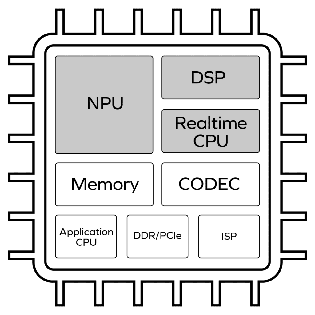
It’s important to briefly touch on the responsibilities of several of these key building blocks that impact the ML performance of an SoC:
An NPU accelerates compute-intensive, matrix-math ML workloads. NPUs are optimized to handle matrix multiplication blazingly fast but usually cannot run any code other than the ML graph code they were specifically optimized to run. Most NPUs today are essentially large arrays of hardwired, fixed-point multiply-accumulate (MAC) blocks running in parallel. Most NPUs in silicon today can only support a few dozen common neural network operators (or “graph layers”) – a handful each of convolution, pooling, and activation layers – among hundreds of operator types backed by the leading training frameworks such as Tensorflow and PyTorch.
The graph layers running on the NPU usually comprise 90-95%of the expected compute cycles consumed in today’s most popular ML networks, and thus these ML accelerators do an admirable job of handling today’s known inference workloads. Other less performance-critical operators are partitioned to run on the other processor engines in the system, delivering acceptable system performance at the cost of upfront engineering effort. These accelerator NPUs cannot run all layer types – and are not fully programmable processors- therefore they likely cannot run new layers that have not yet been invented by the data scientists who continue to rapidly evolve the state-of-the-art of machine learning. For layers that don’t run on the NPU, the existing approach to delegate these layers to other cores in the system is typically a manual and time-consuming partitioning problem that demands the software programmer have an intimate understanding of the target chip. If a developer needs to target different devices each with a different NPU accelerator, that partitioning exercise needs to be repeated for each new silicon target – a time consuming approach.
DSPs are vector processor cores intended to handle a wide variety of complex math operations efficiently. They are widely used in various applications requiring signal processing – voice or image pre-processing are prime examples.
DSPs can be used to handle some matrix computations, but they are not optimized for them and tend to be inefficient compared to the matrix-optimized NPU accelerators described previously. Additionally, DSPs are typically highly utilized in the system running more conventional C code for signal pre- and post-processing, and thus have little performance headroom to handle heavy matrix computation. Therefore DSPs in most SoCs can augment the NPUs and run some but not all ML graph operators that the NPU doesn’t nativelyh handle.
The realtime CPU is responsible for controlling the overall inference functionality in the SoC. It coordinates ML inference workloads between the NPU, DSP, and the memory (used to store model weights). The realtime CPU is often the only programmable core in the inference subsystem that is exposed to the programmer. Because building and deploying multicore software development kits (SDKs) is a complex task, and because using a multicore SDK requires a complex learning cycle, most semiconductor vendors who employ CPU+DSP+NPU inference subsystems only expose the CPU to the developer for developer code, providing access to the DSP and NPU only via prebuilt application programming interfaces (APIs). If a developer needs an ML operator not supported in the APIs for the NPU or DSP, they can add a new ML operator on the CPU but generally not on the NPU or DSP.
Because CPUs are general purpose, they can functionally run any code the programmer desires, but because they lack the vector performance of a DSP or the matrix performance of an NPU, CPUs are poor performers for new ML operators. The programmer thus must choose between high-performance ML operators prebuilt with published APIs or slow ML operators added to the CPU.
Distinctions must be made between the realtime CPU and an application-class CPU, both of which are shown in the conceptual block diagram above. The latter is the larger CPU core running a complex operating system such as Linux, the application, and many other managerial functions. It usually has little involvement in real-time-sensitive ML computations.
The following are just a few challenges that SoC developers are faced with and how they are presently addressed:
Building SoCs that can handle known challenges is a good start but insufficient. The real challenge is to develop devices that are flexible enough to support some range of future requirements.
ML technology is evolving rapidly. New models, libraries, and operators are introduced at a rapid pace. This makes it essential to develop devices optimized for ML inference that can be programmed to support new operators and algorithms when they become available.
The existing heterogeneous SoC architecture approach described above is often not flexible enough to support new operators with the performance required. This is due to the inflexibility of hardwired NPUs that cannot be reconfigured. Developers tackle this challenge by adding code to the DSP or the realtime CPU to compensate for the NPU’s shortcomings.
This approach is suboptimal in performance and creates a new set of problems. For example, splitting matrix operations between two disparate cores (NPU and CPU) penalizes inference latency and power dissipation since large data blocks have to traverse the chip going from one core to the other.
Dealing with multiple IP cores from multiple IP vendors invariably leads to reliance on multiple toolsets, creating many challenges. It is exceedingly difficult to debug a system using more than one debugger. As an example, it is challenging to find quick answers to common debugging questions such as:
· Where is the system bottleneck?
· Why can’t I get the throughput that I expected?
· Why does inference latency vary so drastically
· Is this problem a software bug or hardware issue?
Presently there are no easy ways to address this problem. Diversity in toolsets invariably leads to longer development times.
Designers need a new AI acceleration processor architecture designed from the ground up to address the significant ML inference deployment challenges facing SoC developers. Quadric’s General Purpose Neural Processing Unit (GPNPU) is a simple yet powerful architecture with demonstrated improved matrix-computation performance than the traditional approach. Its crucial differentiation is its ability to execute diverse workloads with great flexibility all on a single machine.
The Quadric GPNPU is a unified processor architecture that handles matrix operations, vector operations and scalar (control) code in one execution pipeline. These workloads are traditionally handled separately by the NPU, DSP, and real-time CPU. The entire GPNPU architecture is abstracted to the user as a single software-controlled core, allowing for the simple expression of complex parallel workloads.
The Quadric GPNPU is entirely driven by code, empowering developers to continuously optimize the performance of their models and algorithms throughout the device’s lifecycle.
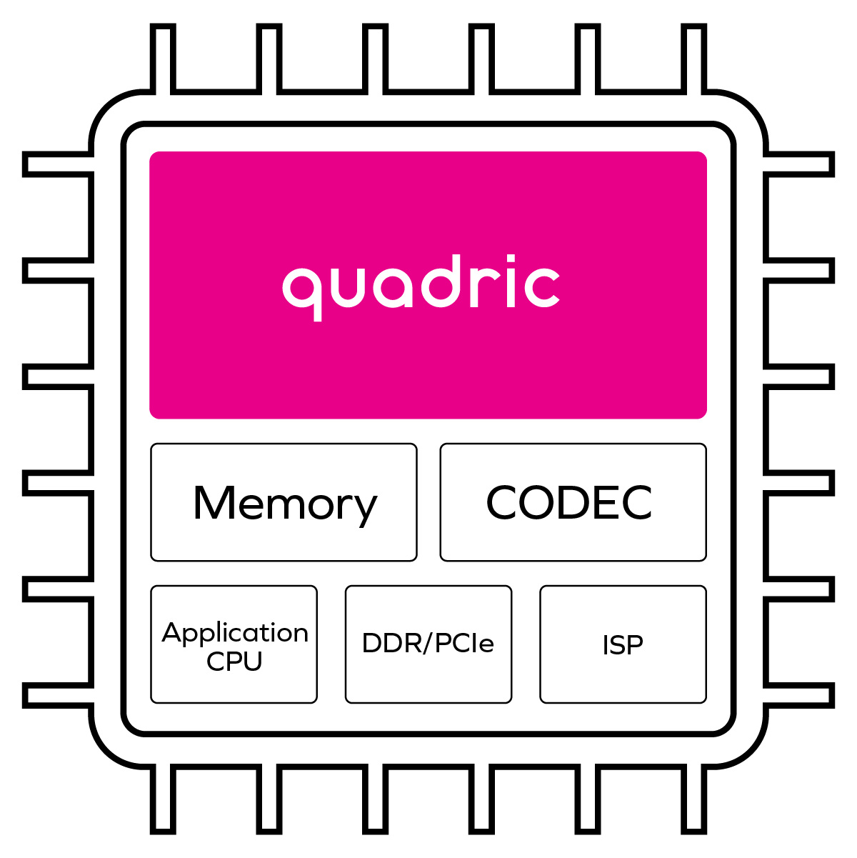
Figure 2 is the conceptual block diagram of the same camera-enabled SoC based on Quadric’s architecture. The significance of this arrangement is that the GPNPU can singlehandedly run workloads traditionally run independently on the DSP, NPU, and real-time CPU cores.
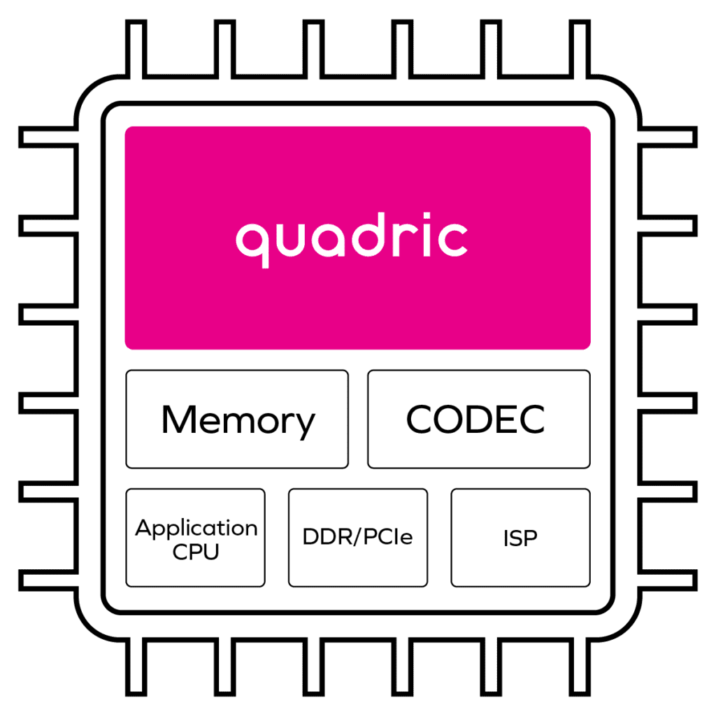
Figure 3 is a comparison of the traditional approach with this new approach based on a GPNPU.
Figure 3. A comparison of the traditional approach (left) and the Quadric GPNPU approach
The benefits of using a GPNPU are:
Quadric’s solution enables hardware developers to instantiate a single core that can handle an entire ML workload plus the typical DSP pre-processing and post-processing, signal conditioning workloads often intermixed with ML inference functions. Dealing with a single core drastically simplifies hardware integration and eases performance optimization. System design tasks such as profiling memory usage to ensure sufficient off-chip bandwidth are greatly simplified.
Quadric’s GPNPU architecture dramatically simplifies software development since matrix, vector, and control code can all be handled in a single code stream. ML graph code from the common training toolsets(Tensorflow, Pytorch, ONNX formats) is compiled by the Quadric toolset and merged with signal processing code written in C++, all compiled into a single code stream running on a single processor core.
Quadric’s toolset meets the demands of both hardware and software developers, who no longer need to master multiple toolsets from multiple vendors. The entire subsystem can be debugged in a single debug console. This dramatically reduces code development time and eases performance optimization.
This new programming paradigm also benefits the end users of the SoCs since they will have access to program all the GPNPU resources.
A Quadric GPNPU can run anything written in C++. This is incredibly powerful since SoC developers can write code to implement new neural network operators and libraries long after the SoC has been taped out. This eliminates fear of the unknown future ML operator and dramatically increases a chip’s useful life.
Again, this flexibility is extended to the end users of the SoCs. They can continuously add new features to the end products, giving them a competitive edge.
Replacing the heterogenous ML subsystem comprised of separate NPU, DSP, and real-time CPU cores with one GPNPU has potent advantages. By allowing vector, matrix, and control code to be handled in a single code stream, the development and debug process is greatly simplified while the ability to add new algorithms efficiently is greatly enhanced.
As ML models continue to evolve and inferencing becomes prevalent in even more applications, the payoff from this unified architecture helps future proof chip design cycles.
© Copyright 2024 Quadric All Rights Reserved Privacy Policy